
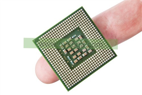
ผู้ผลิต PCB โพรงขั้นบันได
ผู้ผลิต PCB โพรงขั้นบันได,A Step cavity PCB is a specially designed printed circuit board featuring grooves or stepped structures of varying depths on its surface or within its layers. These cavities are used to accommodate components, เศษ, or other elements, allowing for a more compact and high-density circuit layout. Step cavity PCBs find wide applications in high-frequency and microwave circuits, RF applications, และเทคโนโลยีเซ็นเซอร์, offering excellent electromagnetic shielding and signal isolation properties while reducing cross-talk issues in circuits. Their precise design and manufacturing requirements make them integral to many complex electronic devices.
What is a Step cavity PCB?
A Step cavity PCB, also known as a Step-Wedged Vias PCB, is a specialized type of printed circuit board (PCB) designed with stepped cavities or recesses within the board structure. These cavities vary in depth, allowing for precise placement of electronic components or facilitating specific functions such as controlled impedance routing or thermal management.
The design typically involves creating multiple layers within the PCB where the depth of the substrate varies at different points. This variation helps in accommodating components like ICs or semiconductor devices that require specific depth or space considerations. It also aids in reducing the overall thickness of the PCB while maintaining necessary structural integrity and performance.
Step cavity PCBs are often used in high-frequency applications, RF/microwave circuits, and in scenarios where reducing electromagnetic interference (อีเอ็มไอ) and improving signal integrity are crucial. The stepped design allows for better control over signal paths and impedance matching, which is critical for maintaining signal quality in sensitive electronic systems.
Manufacturing Step cavity PCBs involves advanced techniques such as laser drilling, controlled depth milling, or sequential lamination processes to achieve the desired cavity depths and dimensions accurately. These boards are tailored to meet the stringent requirements of modern electronic devices where space, การแสดง, and reliability are paramount.
ผู้ผลิต PCB โพรงขั้นบันได
What are the Step cavity PCB Design Guidelines?
Designing Step cavity PCBs involves several guidelines to ensure optimal performance and manufacturability:
- Layer Arrangement: Plan the layer stack carefully, considering the depth and location of each step cavity relative to other layers. This helps in maintaining structural integrity and signal integrity.
- Cavity Dimensions: Define the dimensions of each cavity precisely, including depth, width, and length, to accommodate components and ensure proper functionality.
- การเลือกวัสดุ: Choose PCB materials suitable for high-frequency applications and thermal management, considering dielectric constant, loss tangent, and thermal conductivity.
- Impedance Control: Ensure controlled impedance for signal integrity by adjusting trace widths, ระยะ ห่าง, and layer thickness around the step cavities.
- ผ่านการออกแบบ: Optimize via placement and size to minimize signal loss and impedance mismatch, especially near step cavity transitions.
- Thermal Considerations: Incorporate thermal vias or heat dissipation structures around cavities to manage heat generated by components effectively.
- ความสามารถในการผลิต: Consult with PCB manufacturers early in the design phase to verify feasibility and optimize manufacturing processes such as laser drilling, depth control, and lamination.
- การทดสอบและการตรวจสอบความถูกต้อง: Perform simulations and prototype testing to validate the design’s electrical performance, พฤติกรรมความร้อน, และความน่าเชื่อถือทางกล.
โดยปฏิบัติตามแนวทางเหล่านี้, designers can create Step cavity PCBs that meet stringent performance requirements for high-frequency and high-reliability applications, ensuring optimal functionality and manufacturability.
What is the Step cavity PCB Fabrication Process?
กระบวนการผลิตสําหรับ Step cavity PCBs involves several key steps to ensure accurate creation of stepped cavities and proper integration of components:
- Design Preparation: Begin with detailed design specifications including layer stack-up, cavity dimensions, การเลือกวัสดุ, and layout considerations for components and vias.
- การเตรียมพื้นผิว: Select and prepare high-quality PCB substrate materials suitable for the desired application, ensuring they meet thermal, electrical, และข้อกําหนดทางกล.
- Layer Alignment and Lamination: Stack and align the PCB layers according to the design, incorporating prepreg layers as needed. Use controlled lamination processes to bond layers together under heat and pressure.
- Cavity Formation: Utilize advanced techniques such as laser drilling or mechanical milling to create stepped cavities within the PCB layers. Ensure precise depth and dimension control to accommodate components accurately.
- Via Drilling and Plating: Drill vias as per design requirements, ensuring proper alignment with signal paths and power planes. Plate vias to establish electrical connections between different layers.
- Trace and Pad Formation: Apply conductive material (usually copper) to define traces and pads according to the PCB layout. Etch away excess copper to form desired circuit patterns.
- เสร็จสิ้นพื้นผิว:Apply a suitable surface finish such as HASL (การปรับระดับบัดกรีลมร้อน), เอนิก (นิกเกิลแช่ทองแบบไม่ใช้ไฟฟ้า), หรือ OSP (สารกันบูดความสามารถในการบัดกรีอินทรีย์) to protect exposed copper surfaces and facilitate soldering.
- Component Assembly: Place and solder electronic components onto the PCB using automated or manual assembly techniques. Ensure precise alignment within step cavities and verify electrical connections.
- การทดสอบและการตรวจสอบ: Conduct electrical testing, รวมถึงการตรวจสอบความต่อเนื่อง, การทดสอบอิมพีแดนซ์, and functionality tests, to verify the PCB’s performance against design specifications. Inspect for defects and ensure quality control measures are met.
- การตกแต่งขั้นสุดท้าย: Trim excess PCB material, apply markings or labels as required, and prepare the PCB for final packaging and shipment.
โดยทําตามขั้นตอนเหล่านี้, manufacturers can produce Step cavity PCBs that meet stringent performance standards for high-frequency applications, ensuring reliability and functionality in complex electronic systems.
How do you manufacture a Step cavity PCB?
Manufacturing a Step cavity PCB involves a precise and methodical process to create the stepped cavities and integrate components effectively:
- Design Preparation: Begin with detailed design specifications, including layer stack-up, cavity dimensions, การเลือกวัสดุ, and component placement considerations. Ensure designs account for thermal management and signal integrity requirements.
- การเลือกวัสดุ: Choose PCB substrate materials based on thermal conductivity, ค่าคงที่ไดอิเล็กทริก, and mechanical strength suitable for high-frequency applications. Select prepreg materials for lamination.
- Layer Stack-up and Preparation:Arrange and prepare PCB layers according to the design. Clean and condition each layer to ensure proper adhesion during lamination.
- Cavity Formation: Utilize advanced techniques such as laser drilling or mechanical milling to create stepped cavities within the PCB layers. Control depth and dimensions precisely to accommodate components.
- เคลือบ:Stack the prepared layers along with prepreg materials as per the design stack-up. Apply heat and pressure in a controlled environment to laminate the layers together, forming a solid PCB structure.
- Via Drilling and Plating: Drill vias in accordance with the design to establish electrical connections between different layers. Plate vias with conductive material (typically copper) to ensure reliable electrical continuity.
- รูปแบบวงจร: Apply a thin layer of copper over the entire PCB surface. Use photolithography and etching processes to define circuit traces and pads according to the PCB layout.
- เสร็จสิ้นพื้นผิว: Apply a suitable surface finish (เช่น, HASL, เอนิก, OSP) to protect exposed copper surfaces from oxidation and facilitate soldering during assembly.
- Component Assembly: Place electronic components into the designated step cavities and solder them onto the PCB. Ensure precise alignment and secure electrical connections.
- การทดสอบและการตรวจสอบ: Perform electrical tests, such as continuity checks and impedance testing, to verify the functionality and performance of the PCB. Inspect for defects using visual inspection and automated testing equipment.
- การตกแต่งขั้นสุดท้าย:Trim excess PCB material, apply markings or labels as required, and perform final quality checks. Prepare the PCB for packaging and shipment to the customer or assembly facility.
โดยทําตามขั้นตอนเหล่านี้, manufacturers can produce Step cavity PCBs that meet stringent quality standards and performance requirements for various high-frequency and high-reliability applications in electronics.
How much should a Step cavity PCB cost?
The cost of Step cavity PCBs can vary widely based on several factors:
- ความซับซ้อนของการออกแบบ: The intricacy of the step cavities, จํานวนชั้น, and overall design complexity significantly impact the cost. More complex designs requiring precise cavity dimensions and multiple layers will generally be more expensive.
- Materials: The choice of PCB substrate materials, prepregs, and surface finishes influences costs. High-performance materials with specific thermal and electrical properties may increase the overall cost.
- Manufacturing Processes: Specialized manufacturing processes such as laser drilling, controlled depth milling, and precise lamination techniques required for Step cavity PCBs can add to the manufacturing cost.
- ปริมาณ:Economies of scale apply, meaning larger production quantities generally lower the per-unit cost due to spreading out fixed costs across more units.
- Additional Features: Any additional features such as impedance control, specific tolerances, and testing requirements can also affect the overall cost.
- ซัพพลายเออร์และที่ตั้ง:Pricing may vary between different PCB manufacturers and regions based on their capabilities, overhead costs, and market competitiveness.
เพื่อให้การประมาณการคร่าวๆ, Step cavity PCBs typically cost more than standard PCBs due to their specialized design and manufacturing requirements. Prices can range from a few dollars to tens or even hundreds of dollars per board, ขึ้นอยู่กับปัจจัยข้างต้น. เพื่อการกําหนดราคาที่ถูกต้อง, it’s advisable to consult with PCB manufacturers directly, providing detailed specifications of your design and quantity requirements.
What is Step cavity PCB base material?
The base material used for Step cavity PCBs is typically chosen based on the specific requirements of the application, เช่นประสิทธิภาพความถี่สูง, การจัดการความร้อน, และความแข็งแรงเชิงกล. Common base materials include:
- FR-4 (สารหน่วงไฟ 4): This is a widely used epoxy-based laminate and prepreg material known for its good electrical insulation properties and cost-effectiveness. FR-4 is suitable for many standard PCB applications but may not always meet the stringent requirements of high-frequency designs without additional modifications.
- ลามิเนตความถี่สูง: Specialized laminates such as Rogers RO4000 series, Taconic, or Isola’s high-frequency materials are designed to provide excellent electrical performance at higher frequencies. These materials often have lower dielectric constants, lower loss tangents, and improved thermal stability compared to FR-4.
- Thermally Conductive Substrates: For applications requiring effective thermal management, substrates with high thermal conductivity are used. Materials like metal core PCBs (MCPCB) or thermally conductive dielectric materials are chosen to dissipate heat generated by components efficiently.
- Ceramic-Based Materials: In some cases, ceramic-based materials such as Alumina (Al₂O₃) or Aluminum Nitride (อัลเอ็น) are used for their excellent thermal conductivity and reliability in high-temperature environments. These materials are suitable for applications requiring superior thermal performance and reliability.
The choice of base material depends on factors such as operating frequency, thermal requirements, เสถียรภาพทางกล, and cost considerations. Designers and engineers select the material that best meets the specific performance and reliability requirements of their Step cavity PCB designs.
Which company makes Step cavity PCBs?
Several companies are capable of manufacturing Step cavity PCBs, which require highly precise processes and technologies. เช่น, companies like Rogers Corporation, อิโซลา กรุ๊ป, and Taconic Advanced Dielectric Division are renowned for their specialized high-frequency laminate materials used extensively in microwave and high-frequency circuit applications. These companies employ advanced techniques and materials to meet the manufacturing requirements of Step cavity PCBs, ensuring complex designs and maintaining high-frequency performance and stability.
นอกจากนี้, various high-tech electronic companies, both domestically and internationally, focus on producing high-performance PCBs and can offer customized solutions for Step cavity PCBs. These manufacturers typically possess advanced production equipment and extensive experience to manufacture intricate PCB structures according to specific customer requirements.
As for our company, we have the capability and experience to manufacture Step cavity PCBs. Equipped with advanced PCB manufacturing equipment and a skilled technical team, we handle complex design requirements and high-performance electronic applications. We prioritize quality control and offer customized services to meet the exact design specifications and performance requirements of our customers.
Whether in material selection, กระบวนการผลิต, or quality assurance, we are committed to meeting high standards. If you have specific requirements for Step cavity PCBs or would like more detailed information, please feel free to contact us. We are dedicated to providing professional technical support and service.
What are the qualities of good customer service?
Good customer service encompasses several key qualities that contribute to a positive experience for customers:
- ตอบ สนอง: Being prompt in addressing customer inquiries, เกี่ยว ข้อง กับ, and requests demonstrates attentiveness and respect for their time.
- ความเห็นอกเห็นใจ: Understanding and empathizing with the customer’s perspective shows care and builds rapport. It involves actively listening to their needs and concerns.
- ความชัดเจน: Providing clear and concise information helps customers understand solutions, policies, and next steps easily.
- ความอดทน: Remaining patient, especially when dealing with complex issues or frustrated customers, fosters a supportive and calming interaction.
- มือ อาชีพ: Maintaining a professional demeanor and language ensures credibility and trustworthiness in resolving issues.
- ความรู้: Having in-depth knowledge of products, บริการ, and policies enables effective problem-solving and enhances credibility.
- Proactivity: Anticipating customer needs and offering relevant suggestions or solutions before issues arise demonstrates initiative and care.
- Efficiency: Resolving issues swiftly and effectively shows respect for the customer’s time and enhances satisfaction.
- Personalization: Tailoring interactions based on individual customer preferences and history fosters a personalized and memorable experience.
- Follow-up: Following up after resolving an issue or completing a transaction reinforces care and ensures customer satisfaction.
โดยรวบรวมคุณสมบัติเหล่านี้, businesses can cultivate strong customer relationships, encourage loyalty, and differentiate themselves in competitive markets.
FAQs about Step cavity PCBs
What are Step cavity PCBs?
Step cavity PCBs are specialized printed circuit boards designed with stepped cavities or recesses within the board structure. These cavities vary in depth, allowing for precise placement of components or facilitating specific functions such as controlled impedance routing or thermal management.
Where are Step cavity PCBs used?
Step cavity PCBs are used in various high-performance applications such as telecommunications, อวกาศ, อุปกรณ์ทางการแพทย์, and high-frequency RF/microwave circuits where stringent performance and reliability are critical.
How are Step cavity PCBs manufactured?
Manufacturing involves advanced techniques like laser drilling or mechanical milling to create stepped cavities within PCB layers. Precise control of cavity dimensions and layer alignment is crucial for optimal performance.
What materials are used for Step cavity PCBs?
Common materials include high-frequency laminates like Rogers RO4000 series, Isola’s high-performance materials, and thermally conductive substrates for enhanced thermal management.
What design considerations are important for Step cavity PCBs?
Key considerations include layer stack-up, cavity dimensions, material selection for thermal and electrical properties, and ensuring proper impedance control and signal integrity.
Can Step cavity PCBs be customized?
Yes, Step cavity PCBs can be customized to meet specific application requirements, including cavity dimensions, การเลือกวัสดุ, and performance specifications tailored to the application’s needs.