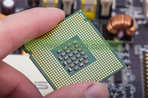
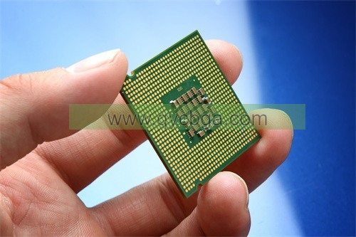
What is Semiconductor Package Substrate?
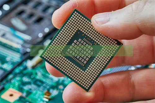
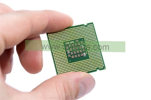
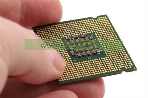
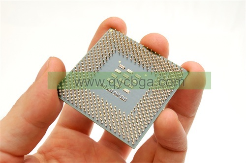
Производитель подложек для полупроводниковых корпусов,A semiconductor package substrate is a critical component in microelectronics, providing the foundational platform for mounting and interconnecting semiconductor chips. These substrates are designed with multiple layers of conductive traces and insulating materials, ensuring reliable electrical performance and signal integrity. They offer excellent thermal dissipation, mechanical support, and protection for the delicate semiconductor devices. Commonly made from materials like BT resin, ceramics, or organic substrates, they cater to various applications, including computing, telecommunications, и автомобильной электроники. Semiconductor package substrates enable miniaturization and high-density integration, making them essential for advanced electronic devices requiring high performance, durability, and efficient heat management.
The substrate is typically made of a thin, flat material such as ceramic or organic laminate, which has been coated with conductive traces and pads. These traces and pads form the electrical pathways that allow signals to flow between the die and the external components of the electronic system, such as other ICs, printed circuit boards (Печатные платы), or connectors.
There are several types of semiconductor package substrates, each with its own characteristics and advantages. Some common types include:
- Ceramic substrates: These are made of materials like alumina (Ал2О3) или нитрид алюминия (AlN) and are known for their excellent thermal conductivity and mechanical strength. Ceramic substrates are often used in high-performance applications where thermal management is critical.
- Organic substrates: These are made of organic materials such as epoxy resin reinforced with fiberglass (ФР-4) or other substrates like BT (bismaleimide triazine). Organic substrates are less expensive than ceramic substrates and are commonly used in consumer electronics and other cost-sensitive applications.
- Leadframe-based substrates: These substrates use a leadframe structure made of metal (typically copper or copper alloy) to provide both electrical connections and mechanical support for the die. Leadframe-based substrates are often used in semiconductor packages such as quad flat packages (QFPs) and small outline integrated circuits (SOICs).
- Package-on-Package (PoP) substrates: These substrates are used in PoP configurations where multiple semiconductor packages are stacked on top of each other to save space and improve performance. PoP substrates typically feature advanced interconnect technologies such as through-silicon vias (TSVs) to enable vertical stacking of chips.
Полный, the choice of substrate depends on factors such as the electrical performance requirements, thermal management needs, Соображения по стоимости, and the specific application of the semiconductor package.

Производитель подложек для полупроводниковых корпусов
Semiconductor Package Substrate design Reference Guide.
Designing a semiconductor package substrate requires careful consideration of various factors to ensure optimal performance, надёжность, и технологичность. Here’s a reference guide outlining key considerations and best practices:
- Электрические характеристики:
– Signal integrity: Ensure controlled impedance for signal traces to minimize signal degradation and electromagnetic interference.
– Power delivery: Design power distribution network (ПДН) with low impedance paths to efficiently deliver power to the die.
– Crosstalk mitigation: Implement proper spacing and shielding techniques to minimize crosstalk between signal traces.
– High-speed design: Use transmission line structures and impedance matching techniques for high-speed interfaces to maintain signal integrity.
- Управление температурным режимом:
– Thermal vias: Incorporate thermal vias to facilitate heat dissipation from the die to the substrate and ultimately to the PCB or heat sink.
– Thermal conductivity: Choose substrate materials with high thermal conductivity, such as ceramics or metal-core laminates, to enhance heat transfer.
– Thermal relief: Design thermal relief patterns to minimize thermal stress on the die during temperature cycling.
– Heat spreaders: Consider integrating heat spreaders or heat sinks into the substrate design to further enhance thermal performance.
- Mechanical Considerations:
– Die attach: Design appropriate pads or lands for die attach and ensure proper alignment and bonding during assembly.
– Package warpage: Minimize substrate warpage to ensure compatibility with surface mount assembly processes and to prevent reliability issues.
– Package size and thickness: Optimize package dimensions to meet mechanical requirements while maintaining compatibility with assembly equipment and system form factors.
- Технологичность:
– Design for manufacturability (DFM): Follow DFM guidelines to simplify fabrication processes, reduce manufacturing costs, and improve yield.
– Panelization: Arrange substrate designs on manufacturing panels efficiently to maximize throughput during fabrication.
– Assembly compatibility: Ensure compatibility with standard assembly processes, such as solder paste printing, pick-and-place, and reflow soldering.
– Testability: Incorporate test points and access features into the substrate design to facilitate electrical testing and inspection.
- Reliability and Quality:
– Material selection: Choose substrate materials with suitable mechanical and thermal properties to ensure long-term reliability in the intended operating environment.
– Environmental robustness: Design for resistance to environmental factors such as moisture, влажность, and thermal cycling to ensure reliability over the product’s lifecycle.
– Failure analysis: Implement features for failure analysis and debugging, such as traceability markings and accessible test points.
By carefully addressing these considerations and leveraging industry standards and best practices, semiconductor package substrate designers can develop robust and high-performance substrates that meet the requirements of a wide range of applications. Collaboration with semiconductor manufacturers, assembly partners, and component suppliers can further enhance the design process and ensure successful product realization.
What are the materials used in Semiconductor Package Substrate?
Semiconductor package substrates can be made from various materials, each offering different properties and advantages. Some common materials used in semiconductor package substrates include:
- Ceramics: Ceramics such as alumina (Ал2О3) и нитрид алюминия (AlN) are known for their excellent thermal conductivity, механическая прочность, и надежность. These properties make ceramics ideal for high-power and high-frequency applications where thermal management is critical.
- Organic laminates: Organic substrates, typically made from epoxy resin reinforced with fiberglass (ФР-4), are widely used in consumer electronics and other cost-sensitive applications. Organic laminates offer good electrical insulation, ease of fabrication, and low cost. Однако, they generally have lower thermal conductivity compared to ceramics.
- Metal-core laminates: Metal-core laminates feature a thin layer of metal (например., aluminum or copper) sandwiched between layers of organic material. These substrates provide better thermal conductivity than standard organic laminates while still offering ease of fabrication and cost-effectiveness.
- Leadframes: Leadframes are made of metal (usually copper or copper alloy) and provide both electrical connections and mechanical support for the semiconductor die. Leadframes are commonly used in packages such as quad flat packages (QFPs) and small outline integrated circuits (SOICs).
- Flexible substrates: Flexible substrates, often made from materials like polyimide, offer flexibility and versatility for applications where bendability or conformal packaging is required. Flexible substrates are commonly used in applications such as flexible printed circuit boards (Печатные платы) and wearable electronics.
- Copper core substrates: Copper core substrates feature a core layer of copper for enhanced thermal conductivity, surrounded by layers of dielectric material. These substrates are suitable for high-power applications where efficient heat dissipation is essential.
- Copper-invar-copper (CIC) substrates: CIC substrates consist of layers of copper and invar (a nickel-iron alloy) bonded together. These substrates offer excellent thermal expansion matching with semiconductor dies, reducing the risk of thermal stress-induced failures.
The choice of substrate material depends on various factors, including electrical performance requirements, thermal management needs, mechanical constraints, Соображения по стоимости, and the specific application of the semiconductor package. Each material has its own set of advantages and limitations, and the selection process involves balancing these factors to achieve the desired performance and reliability.
How is Semiconductor Package Substrate manufactured?
The manufacturing process for semiconductor package substrates involves several steps, including substrate fabrication, surface preparation, circuit patterning, металлизация, and final assembly. Ниже приведен обзор типичного производственного процесса:
- Изготовление подложек:
– The manufacturing process begins with the fabrication of the substrate material, which could be ceramic, organic laminate, metal-core laminate, or another suitable material.
– For ceramic substrates, the process may involve forming green sheets from ceramic powders, followed by stacking and bonding the sheets to create the desired substrate thickness.
– Organic substrates are typically produced by laminating layers of epoxy resin and fiberglass, which are then cured to form a solid substrate.
– Metal-core substrates are manufactured by bonding a thin layer of metal (например., aluminum or copper) between layers of organic material.
- Подготовка поверхности:
– Once the substrate material is prepared, the surface is cleaned and treated to ensure proper adhesion of subsequent layers.
– Surface treatment techniques may include chemical cleaning, plasma treatment, or mechanical abrasion, depending on the substrate material and specific manufacturing requirements.
- Circuit Patterning:
– The substrate surface is coated with a layer of photoresist, which is then exposed to ultraviolet (UV) light through a photomask containing the desired circuit pattern.
– После воздействия, the photoresist is developed to remove the unexposed areas, leaving behind the patterned photoresist mask.
- Металлизация:
– The substrate undergoes a metallization process to deposit conductive traces and pads onto the patterned surface.
– Metallization techniques may include sputtering, evaporation, гальванопокрытие, or chemical vapor deposition (ССЗ), depending on the substrate material and metallization requirements.
– After metallization, the remaining photoresist mask is stripped away, leaving behind the patterned conductive traces and pads on the substrate surface.
- Final Assembly:
– Once the conductive traces and pads are formed, the substrate is ready for final assembly.
– Semiconductor dies are attached to the substrate using die attach materials such as epoxy or solder.
– Wire bonding or flip-chip bonding techniques are used to connect the bond pads on the die to the corresponding pads on the substrate.
– Additional assembly steps may include encapsulation with molding compound, leadframe attachment (for leadframe-based packages), and surface finishing processes such as solder mask application and surface plating.
На протяжении всего производственного процесса, quality control measures are implemented to ensure the dimensional accuracy, Электрические характеристики, and reliability of the semiconductor package substrates. This may involve inspection, testing, and validation at various stages of production to identify and correct any defects or deviations from specifications.
The Application area of Semiconductor Package Substrate
Semiconductor package substrates find application across a wide range of industries and electronic devices. Некоторые из ключевых областей применения включают:
- Электроника:
– Smartphones, Таблетки, Ноутбуки, and wearable devices often incorporate semiconductor package substrates in their circuitry. These substrates enable the integration of high-performance semiconductor chips into compact and portable devices.
- Автомобильная электроника:
– Advanced driver-assistance systems (АДАС), infotainment systems, engine control units (Экю), and other automotive electronics rely on semiconductor package substrates for their functionality. These substrates provide the necessary electrical connections and thermal management for reliable operation in harsh automotive environments.
- Industrial Electronics:
– Industrial automation, robotics, instrumentation, and control systems utilize semiconductor package substrates for various applications. These substrates enable the implementation of complex electronic circuits in industrial equipment, ensuring reliability and performance in demanding industrial environments.
- Telecommunications:
– Telecommunication infrastructure equipment, such as base stations, routers, and switches, utilize semiconductor package substrates in their circuitry. These substrates support high-speed data processing and communication functions critical for modern telecommunications networks.
- Медицинские приборы:
– Medical imaging equipment, patient monitoring systems, implantable devices, and diagnostic instruments rely on semiconductor package substrates for their electronic components. These substrates facilitate precise control and measurement capabilities essential for medical diagnostics and treatment.
- Аэрокосмическая и оборонная промышленность:
– Aerospace and defense applications, including avionics, radar systems, satellites, and military vehicles, utilize semiconductor package substrates for their electronic systems. These substrates must meet stringent reliability and performance requirements to operate in challenging aerospace and defense environments.
- Networking and Data Centers:
– Networking equipment, data center servers, and storage systems incorporate semiconductor package substrates in their circuitry. These substrates enable high-speed data processing and transmission, supporting the increasing demands of modern networking and cloud computing infrastructure.
- Renewable Energy:
– Renewable energy systems, such as solar inverters, wind turbines, и системы накопления энергии, utilize semiconductor package substrates for power conversion and control functions. These substrates play a crucial role in optimizing energy efficiency and managing power generation and distribution in renewable energy applications.
Полный, semiconductor package substrates serve as essential components in a wide range of electronic devices and systems, enabling the integration of semiconductor chips and providing the necessary electrical, термический, and mechanical support for reliable operation in various industries and applications.
What are the advantages of Semiconductor Package Substrate?
Semiconductor package substrates offer several advantages that make them essential components in electronic devices and systems. Некоторые из ключевых преимуществ включают в себя:
- Electrical Connectivity: Semiconductor package substrates provide a platform for connecting semiconductor chips (dies) to the rest of the electronic system. They feature conductive traces and pads that facilitate electrical connections between the die and other components, such as integrated circuits (HCR), printed circuit boards (Печатные платы), и разъемы.
- Миниатюризация: Package substrates enable the integration of semiconductor chips into compact and lightweight electronic devices. By providing a compact and dense layout for connecting multiple chips and components, substrates contribute to the miniaturization of electronic systems, making them more portable and space-efficient.
- Управление температурным режимом: Substrates play a crucial role in managing the heat generated by semiconductor chips during operation. They facilitate heat dissipation from the die to the surrounding environment, helping to maintain optimal operating temperatures and prevent thermal stress-related failures. Substrates made from materials with high thermal conductivity, such as ceramics or metal-core laminates, offer superior thermal management capabilities.
- Mechanical Support: Semiconductor package substrates provide mechanical support and protection for semiconductor chips, ensuring their proper alignment and structural integrity within the electronic system. They help to prevent damage to the chips from mechanical shocks, Вибрации, and other environmental stresses encountered during operation and handling.
- Настройка: Substrate designs can be customized to meet the specific requirements of different semiconductor packages and applications. Design flexibility allows for the integration of various features, such as different numbers and configurations of electrical connections, thermal vias, and mounting options, to accommodate diverse performance and form factor requirements.
- Cost Efficiency: Package substrates offer cost-effective solutions for connecting semiconductor chips in electronic systems. They are typically produced using high-volume manufacturing processes and materials, resulting in relatively low unit costs compared to alternative packaging technologies. Дополнительно, substrates contribute to overall cost savings by enabling the integration of multiple functions and components into a single package.
- Надёжность: Semiconductor package substrates are designed and manufactured to meet stringent reliability standards, ensuring the long-term performance and durability of electronic systems. They undergo rigorous testing and quality control measures to identify and eliminate potential defects, minimizing the risk of premature failures and ensuring the reliability of the end products.
Полный, semiconductor package substrates play a critical role in enabling the functionality, performance, and reliability of electronic devices and systems across various industries and applications. Their advantages in electrical connectivity, Управление температурным режимом, mechanical support, customization, cost efficiency, and reliability make them indispensable components in modern electronic design and manufacturing.
How Much Does Semiconductor Package Substrate Cost?
The cost of semiconductor package substrates can vary significantly depending on various factors, including the substrate material, размер, complexity, Производственные процессы, Требования к кастомизации, and market conditions. Вообще, the cost of semiconductor package substrates is influenced by the following factors:
- Материал основания: Different substrate materials have varying costs associated with their production. Например, ceramic substrates tend to be more expensive than organic laminates due to their higher thermal conductivity and mechanical strength.
- Size and Complexity: Larger and more complex substrate designs with dense circuitry, multiple layers, and advanced features such as high-speed signal routing or thermal management structures may incur higher manufacturing costs.
- Производственные процессы: The cost of manufacturing semiconductor package substrates is influenced by the complexity of the fabrication processes involved, such as photolithography, металлизация, and assembly. Advanced manufacturing techniques and equipment may increase production costs.
- Настройка: Customized substrate designs tailored to specific performance or form factor requirements may involve additional engineering and manufacturing costs compared to standard off-the-shelf substrates.
- Volume and Economy of Scale: Large-volume production runs typically benefit from economies of scale, resulting in lower per-unit manufacturing costs. Однако, smaller production runs or low-volume applications may incur higher unit costs due to setup and tooling expenses.
- Market Conditions: Market dynamics, including supply and demand fluctuations, material availability, and competitive pricing pressure, can influence the cost of semiconductor package substrates.
While it’s challenging to provide specific cost figures without considering these factors and industry-specific details, semiconductor package substrate costs can range from a few cents to several dollars per unit, depending on the aforementioned factors. For precise pricing information, it’s advisable to consult with substrate manufacturers or suppliers and request a quotation based on your specific requirements and volume expectations.
ЧАСТО ЗАДАВАЕМЫЕ ВОПРОСЫ
What is a semiconductor package substrate?
A semiconductor package substrate is a material layer that provides electrical connections, Управление температурным режимом, and mechanical support for semiconductor chips within electronic devices.
What materials are used to make semiconductor package substrates?
Semiconductor package substrates can be made from various materials, including ceramics (such as alumina or aluminum nitride), organic laminates (например., epoxy resin reinforced with fiberglass), metal-core laminates, leadframes, and flexible substrates (например., polyimide).
What are the advantages of semiconductor package substrates?
Some advantages of semiconductor package substrates include electrical connectivity, миниатюризация, Управление температурным режимом, mechanical support, customization, cost efficiency, и надежность.
How are semiconductor package substrates manufactured?
The manufacturing process for semiconductor package substrates typically involves substrate fabrication, surface preparation, circuit patterning, металлизация, and final assembly. Each step involves specific techniques and processes tailored to the substrate material and design requirements.
What are the application areas of semiconductor package substrates?
Semiconductor package substrates find application across various industries and electronic devices, including consumer electronics, Автомобильная электроника, industrial equipment, telecommunications, Медицинские приборы, aerospace and defense systems, Сети, data centers, and renewable energy systems.
How much does a semiconductor package substrate cost?
The cost of semiconductor package substrates varies depending on factors such as substrate material, размер, complexity, Производственные процессы, Требования к кастомизации, volume, and market conditions. Costs can range from a few cents to several dollars per unit.
What factors should be considered when selecting a semiconductor package substrate?
When selecting a semiconductor package substrate, factors to consider include electrical performance, thermal management capabilities, механическая прочность, customization options, стоить, надёжность, and compatibility with the specific application and environmental conditions.
 Производитель подложек для упаковки FCBGA

