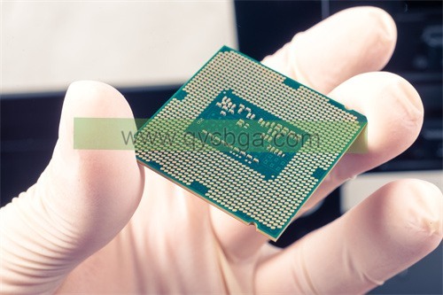
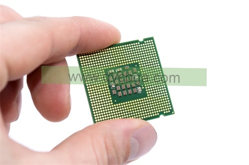
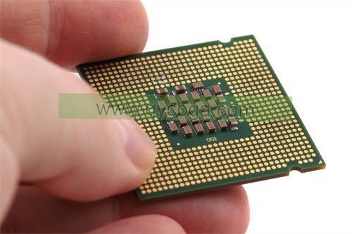
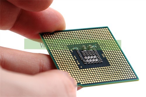
Что такое подложка для упаковки LCC?
Производитель подложек для упаковки LCC,LCC (Безвыводный держатель стружки) package substrate is a compact and versatile semiconductor packaging solution. This substrate features a flat surface with conductive pads for chip attachment, eliminating the need for traditional leads. LCC substrates offer efficient heat dissipation and reliable electrical connections, making them suitable for high-density applications. They are commonly used in telecommunications, automotive, and consumer electronics where space-saving and performance are paramount. LCC package substrates are typically made from materials like ceramic or high-performance organic laminates, ensuring durability and stability in harsh operating environments. Their simplicity and reliability make LCC substrates a preferred choice for modern electronic assemblies.
The LCC (Безвыводный держатель стружки) package substrate is a type of electronic packaging used to mount and interconnect интегральные схемы (HCR) onto printed circuit boards (Печатные платы). LCC packages are designed to be compact and provide a high level of electrical performance while being compatible with surface mount technology (СМТ) Сборочные процессы.
The substrate in an LCC package serves as a platform for the integrated circuit and provides electrical connections between the IC and the PCB. It typically consists of a thin layer of insulating material, such as fiberglass-reinforced epoxy resin (ФР-4), with conductive traces and pads etched onto its surface. These traces and pads allow for the transfer of electrical signals between the IC and the rest of the circuit.
One of the distinguishing features of the LCC package is its lack of leads (hence the term “leadless”). Instead of traditional leads, LCC packages utilize metal pads on the bottom surface of the package that make direct contact with corresponding pads on the PCB. This design helps to reduce the overall size of the package and can improve electrical performance by minimizing parasitic effects associated with leaded packages.
Полный, LCC package substrates are commonly used in a variety of electronic applications where space savings, высокая производительность, and compatibility with SMT assembly processes are important considerations.

Производитель подложек для упаковки LCC
LCC Package Substrate design Reference Guide.
A comprehensive reference guide specifically dedicated to the design of LCC package substrates might be a bit niche, but you can find valuable information in various sources such as technical documentation, application notes from semiconductor manufacturers, and industry publications. Here’s a general outline of what you might find in such a guide:
- Introduction to LCC Packages: This section would provide an overview of LCC packages, their advantages, Приложений, and key features.
- Выбор материала основания: Discuss different substrate materials suitable for LCC packages, including FR-4, high-temperature laminates, and other advanced materials. Explain the considerations for material selection such as thermal properties, Электрические характеристики, and cost.
- Substrate Design Guidelines: Offer guidelines for designing the substrate layout, including pad placement, trace routing, via placement, and layer stack-up. This section would address considerations such as signal integrity, Распределение питания, and thermal management.
- Electrical Performance Considerations: Discuss techniques for optimizing electrical performance, including impedance control, signal integrity analysis, and minimizing parasitic effects.
- Управление температурным режимом: Cover strategies for managing heat within the package, including thermal vias, Радиаторы, and thermal pads. Explain thermal modeling techniques and considerations for high-power applications.
- Manufacturing and Assembly Guidelines: Provide recommendations for designing substrates that are manufacturable and compatible with standard assembly processes such as surface mount technology (СМТ) and reflow soldering.
- Reliability and Testing: Discuss reliability considerations such as solder joint reliability, mechanical stress, and environmental testing. Provide guidelines for reliability testing and qualification.
- Тематические исследования и примеры: Include real-world examples of LCC package substrate designs, Выделение лучших практик, Возникшие проблемы, and solutions implemented.
- References and Resources: Provide a list of references, standards, and additional resources for further reading and research.
While there may not be a single comprehensive guide dedicated solely to LCC package substrate design, you can find valuable information by consulting multiple sources and leveraging the expertise of semiconductor manufacturers, industry organizations, and technical publications.
What are the materials used in LCC Package Substrate?
The materials used in LCC (Безвыводный держатель стружки) package substrates typically include:
- Материал основания: The main body of the substrate is typically made from an insulating material, most commonly fiberglass-reinforced epoxy resin, commonly known as FR-4. FR-4 offers good electrical insulation properties and mechanical strength, making it suitable for a wide range of electronic applications.
- Conductive Traces and Pads: The conductive traces and pads on the substrate are usually made from copper. Copper is chosen for its excellent electrical conductivity, allowing for efficient signal transmission within the package.
- Паяльная маска: A solder mask layer is applied over the substrate to protect the copper traces from oxidation and to prevent solder bridges during assembly. Solder mask material is typically composed of epoxy resin with pigments added to provide the desired color.
- Обработка поверхности: The surface finish is applied to the exposed copper pads to facilitate soldering during assembly. Common surface finishes for LCC package substrates include electroless nickel immersion gold (ЭНИГ), immersion tin, and immersion silver.
- Dielectric Material: В некоторых случаях, additional dielectric layers may be added to the substrate to provide insulation between different signal layers or to improve signal integrity. These dielectric materials can vary and may include materials such as polyimide or liquid crystal polymer (LCP).
- Optional Materials for Advanced Applications: For high-performance or specialized applications, alternative substrate materials may be used. These could include high-temperature laminates, Керамические подложки, or flexible substrates depending on the specific requirements of the application.
Полный, the choice of materials for LCC package substrates depends on factors such as electrical performance, Управление температурным режимом, стоить, и технологичность, with designers selecting materials that best meet the needs of their particular application.
How is LCC Package Substrate manufactured?
The manufacturing process for LCC (Безвыводный держатель стружки) package substrates involves several steps, including substrate fabrication, металлизация, assembly of components, и тестирование. Вот общий обзор производственного процесса:
- Изготовление подложек:
– Подготовка основания: The process begins with the preparation of the substrate material, typically fiberglass-reinforced epoxy resin (ФР-4). Sheets of FR-4 are cut to the desired size.
– Layer Stacking: Multiple layers of substrate material may be stacked together to create a multilayer substrate. Each layer may have conductive traces and pads etched onto its surface.
– Сверление: Holes are drilled through the substrate where vias are needed to connect different layers.
- Металлизация:
– Copper Deposition: A thin layer of copper is deposited onto the substrate surface using processes such as electroplating or sputtering. This copper layer forms the conductive traces and pads on the substrate.
– Офорт: A photoresist mask is applied to the copper layer, and then the unwanted copper is etched away using chemical processes, leaving behind the desired conductive patterns.
- Нанесение паяльной маски:
– A layer of solder mask material is applied over the substrate, covering the copper traces and pads while leaving openings for soldering.
- Обработка поверхности:
– The exposed copper pads are coated with a surface finish to facilitate soldering during component assembly. Common surface finishes include electroless nickel immersion gold (ЭНИГ), immersion tin, and immersion silver.
- Component Assembly:
– Placement of Components: Surface mount components, в том числе интегральные схемы (HCR), resistors, capacitors, and other electronic components, are placed onto the substrate using pick-and-place machines.
– Soldering: The components are soldered onto the substrate using reflow soldering or wave soldering processes. In reflow soldering, solder paste is applied to the pads, and then the entire assembly is heated to melt the solder, forming electrical connections between the components and the substrate.
- Испытания и инспекция:
– The assembled substrates undergo testing and inspection to ensure that all components are properly connected and that there are no defects or soldering issues.
– Various testing methods may be employed, including electrical testing to verify connectivity and functionality, Визуальный осмотр, and automated optical inspection (AOI) to check for defects.
- Окончательная упаковка:
– Once testing is complete and any necessary repairs or rework have been performed, the substrates may be packaged and shipped to customers or further integrated into larger electronic assemblies.
На протяжении всего производственного процесса, quality control measures are implemented to ensure that the substrates meet the required specifications and standards for performance and reliability.
The Application area of LCC Package Substrate
LCC (Безвыводный держатель стружки) package substrates find application across a wide range of industries and electronic devices where compact size, высокая производительность, and reliability are essential. Some common application areas include:
- Электроника: LCC package substrates are commonly used in various consumer electronic devices such as smartphones, Таблетки, Ноутбуки, digital cameras, and portable media players. These substrates enable the integration of high-performance ICs in compact form factors, contributing to the sleek design and functionality of consumer gadgets.
- Telecommunications: In the telecommunications industry, LCC package substrates are utilized in networking equipment, routers, switches, base stations, and other communication devices. They facilitate the implementation of high-speed data processing, Маршрутизация сигналов, and wireless connectivity features essential for telecommunications infrastructure.
- Автомобильная электроника: LCC package substrates are employed in automotive electronic systems for applications such as engine control units (Экю), infotainment systems, advanced driver-assistance systems (АДАС), and in-vehicle networking. These substrates provide reliable performance in harsh automotive environments, withstanding temperature variations, Вибрации, and moisture.
- Industrial Electronics: LCC package substrates are used in various industrial applications, including automation systems, control panels, Моторные приводы, power supplies, and instrumentation equipment. They enable the integration of sophisticated control and monitoring functions in industrial environments while meeting stringent reliability and performance requirements.
- Медицинские приборы: LCC package substrates are found in medical devices such as diagnostic equipment, patient monitoring systems, imaging devices, и имплантируемые медицинские устройства. These substrates support the implementation of advanced signal processing, data acquisition, and wireless communication features critical for medical applications.
- Аэрокосмическая и оборонная промышленность: LCC package substrates are employed in aerospace and defense applications, including avionics systems, satellite communication systems, radar systems, и системы наведения ракет. They provide high reliability, performance, and ruggedness required for mission-critical applications in challenging environments.
- Промышленная автоматизация: In industrial automation and robotics, LCC package substrates are used in controllers, motion control systems, robotic arms, and sensor interfaces. They enable precise control, real-time communication, and integration with various sensors and actuators in industrial automation applications.
- Renewable Energy: LCC package substrates are utilized in power electronics for renewable energy systems such as solar inverters, wind turbine controllers, и системы накопления энергии. They support efficient power conversion, monitoring, and control functions essential for renewable energy generation and integration into the electrical grid.
Полный, Универсальность, compactness, and reliability of LCC package substrates make them suitable for a wide range of applications across industries where advanced electronic functionality is required.
What are the advantages of LCC Package Substrate?
LCC (Безвыводный держатель стружки) package substrates offer several advantages, making them a popular choice for various electronic applications:
- Compact Size: LCC packages are designed to be compact, with a small footprint compared to traditional leaded packages. This compact size enables the integration of high-density electronic components into space-constrained applications, contributing to the miniaturization of electronic devices.
- High Electrical Performance: LCC package substrates provide excellent electrical performance, with low parasitic effects and high-speed signal transmission capabilities. This makes them suitable for high-frequency applications requiring precise signal integrity and low noise levels.
- Управление температурным режимом: LCC packages typically feature efficient thermal management capabilities, allowing for effective dissipation of heat generated by integrated circuits. This helps prevent overheating and ensures the reliable operation of electronic devices, particularly in high-power applications.
- Compatibility with Surface Mount Technology (СМТ): LCC packages are compatible with surface mount technology (СМТ) Сборочные процессы, making them easy to integrate into modern manufacturing workflows. This compatibility streamlines the assembly process, reduces manufacturing costs, and enables high-volume production.
- Повышенная надежность: LCC package substrates offer improved reliability compared to traditional leaded packages due to their robust design and construction. They are less susceptible to mechanical stress and thermal cycling, reducing the risk of solder joint failures and ensuring long-term performance in demanding environments.
- Enhanced Signal Integrity: The absence of leads in LCC packages reduces parasitic effects such as inductance and capacitance, resulting in improved signal integrity and reduced signal distortion. This is especially beneficial for high-speed digital and analog applications where signal quality is critical.
- Экономичность: LCC packages are often cost-effective compared to other advanced packaging technologies such as ball grid array (BGA) or flip-chip packages. Their simpler design and manufacturing process help lower production costs while still delivering high performance and reliability.
- Versatility: LCC package substrates are versatile and suitable for a wide range of electronic applications across industries, including consumer electronics, telecommunications, automotive, Промышленная автоматизация, аэрокосмический, and defense.
Полный, the advantages of LCC package substrates, including compact size, high electrical performance, thermal management capabilities, compatibility with SMT assembly, надёжность, и экономичность, make them a preferred choice for many electronic designs.
How Much Does LCC Package Substrate Cost?
The cost of LCC (Безвыводный держатель стружки) package substrates can vary depending on several factors, including the complexity of the substrate design, the choice of materials, Производственные процессы, Объем производства, and supplier/vendor pricing. Here are some factors that can influence the cost:
- Substrate Design Complexity: Сложность конструкции подложки, в том числе количество слоев, the density of traces and pads, and any additional features such as impedance control or embedded components, can impact the cost. More complex designs may require specialized manufacturing processes and materials, leading to higher costs.
- Materials Used: The choice of materials for the substrate, such as the type of substrate material (например., ФР-4, high-temperature laminates, керамический), surface finish, solder mask, и диэлектрические материалы, can affect the overall cost. Advanced materials with specific properties may be more expensive than standard materials.
- Производственные процессы: The manufacturing processes involved in producing LCC package substrates, including substrate fabrication, металлизация, assembly of components, и тестирование, contribute to the cost. Complex processes or additional quality control measures may increase production costs.
- Объем производства: The volume of production can significantly impact the cost per unit. Higher volumes typically result in economies of scale, leading to lower per-unit costs. Наоборот, lower production volumes may incur higher costs due to setup fees and lower efficiency.
- Supplier/Vendor Pricing: The pricing policies of substrate manufacturers, suppliers, and vendors can vary based on factors such as market competition, geographic location, and business relationships. Shopping around and obtaining quotes from multiple suppliers can help identify cost-effective options.
Полный, the cost of LCC package substrates can range from a few cents to several dollars per unit, depending on the specific requirements of the application and the factors mentioned above. It’s essential for designers and manufacturers to carefully consider these factors and balance cost considerations with performance, quality, and reliability requirements.
FAQs about LCC Package Substrate
What is an LCC package substrate?
An LCC package substrate is a type of electronic packaging used to mount and interconnect integrated circuits (HCR) onto printed circuit boards (Печатные платы). It features a compact design with metal pads on the bottom surface, eliminating traditional leads.
What are the advantages of LCC package substrates?
LCC package substrates offer advantages such as compact size, high electrical performance, Эффективное управление температурным режимом, compatibility with surface mount technology (СМТ), повышенная надежность, и экономичность.
What materials are used in LCC package substrates?
LCC package substrates typically consist of materials such as fiberglass-reinforced epoxy resin (ФР-4) for the substrate, copper for conductive traces and pads, solder mask for protection, and various surface finishes for soldering.
How are LCC package substrates manufactured?
The manufacturing process for LCC package substrates involves steps such as substrate fabrication, металлизация, Нанесение паяльной маски, surface finish application, component assembly, тестирование, and final packaging.
What applications are LCC package substrates used in?
LCC package substrates find application across industries such as consumer electronics, telecommunications, automotive, Промышленная автоматизация, аэрокосмический, defense, Медицинские приборы, and renewable energy systems.
How much do LCC package substrates cost?
The cost of LCC package substrates can vary depending on factors such as design complexity, materials used, Производственные процессы, Объем производства, and supplier/vendor pricing.
What considerations should be taken into account when designing with LCC package substrates?
Design considerations for LCC package substrates include substrate layout, Целостность сигнала, Управление температурным режимом, manufacturability, надёжность, и совместимость с процессами сборки.
Where can I find more information about LCC package substrates?
Additional information about LCC package substrates can be found in technical documentation, application notes from semiconductor manufacturers, industry publications, and by consulting substrate manufacturers and suppliers.
 Производитель подложек для упаковки FCBGA

