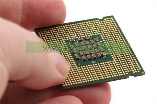
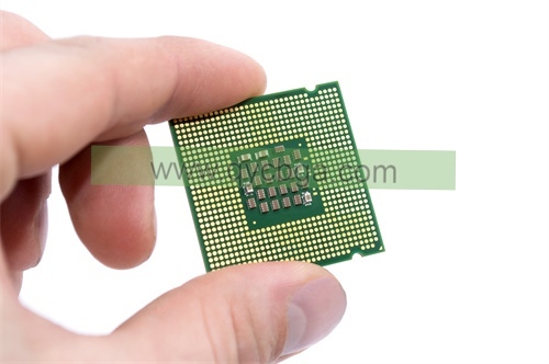
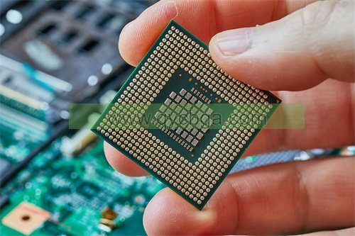
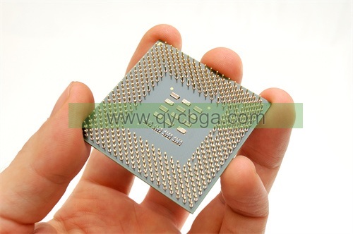
What is FCBGA Package Substrate?
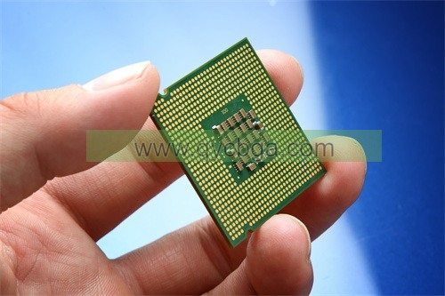
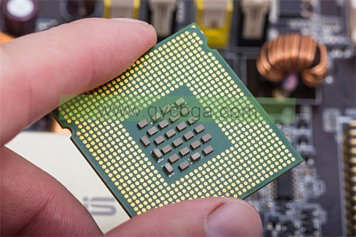
Производитель подложек для упаковки FCBGA,ФКБГА (Массив сетки шаров Flip Chip) package substrate is an advanced semiconductor packaging solution designed for high-performance applications. This substrate features a grid of solder balls on its underside, enabling direct attachment of the semiconductor die using flip chip technology. FCBGA substrates offer superior electrical performance, reduced interconnect length, and efficient thermal dissipation compared to traditional packaging methods. Typically made from materials like organic laminates or ceramics, FCBGA substrates provide robust mechanical support and reliability in harsh operating conditions. Widely used in computing, Сети, and telecommunications, FCBGA package substrates enable compact, high-density electronic assemblies with enhanced performance and reliability.
FCBGA stands for Flip Chip Ball Grid Array, which is a type of packaging technology used in integrated circuits (HCR) like microprocessors and other semiconductor devices. In FCBGA packaging, the silicon die (the actual integrated circuit) is flipped upside down and attached directly to the package substrate using solder bumps.
The package substrate is a thin layer of material (often a laminate or ceramic) with a grid array of metal pads that serve as connection points for the solder balls. These solder balls provide electrical connections between the silicon die and the external circuitry on the printed circuit board (Печатная плата) to which the IC is mounted.
FCBGA packages offer several advantages, включая улучшенные тепловые характеристики, reduced package size, and increased signal integrity compared to other packaging technologies. They are commonly used in high-performance computing applications such as CPUs, GPUs, and networking chips.

Производитель подложек для упаковки FCBGA
FCBGA Package Substrate design Reference Guide.
A comprehensive reference guide for designing FCBGA package substrates typically includes detailed information on various aspects of substrate design, including:
- Выбор материала основания: Guidance on selecting the appropriate substrate material based on factors such as electrical performance, Термические свойства, стоить, and reliability requirements.
- Проектирование стека слоев: Information on designing the layer stackup of the substrate, including the number and arrangement of signal, power, and ground layers, as well as considerations for impedance control and signal integrity.
- Routing Guidelines: Guidelines for routing signal, power, and ground traces on the substrate to minimize signal degradation, переходный разговор, and electromagnetic interference (EMI).
- Проектирование переходных отверстий: Recommendations for via placement, sizing, and design rules to ensure reliable electrical connections between different substrate layers.
- Power Delivery Network (ПДН) Design: Strategies for designing an effective PDN to supply power to the IC, including decoupling capacitor placement and routing of power distribution traces.
- Управление температурным режимом: Techniques for managing thermal performance, such as the design of thermal vias, термопрокладки, and heatsinks to dissipate heat generated by the IC.
- Соображения по производству: Guidelines for designing substrates that are manufacturable, including design rules for fabrication processes such as drilling, plating, and solder mask application.
- Соображения по поводу надежности: Information on designing substrates to meet reliability requirements, including factors such as mechanical stress, solder joint integrity, и термоциклирование.
- Package Design Rules: Specifications for designing the package outline, solder ball array, and other physical features of the FCBGA package.
- Simulation and Analysis Tools: Recommendations for using simulation and analysis tools to evaluate substrate designs for signal integrity, thermal performance, and reliability before fabrication.
A reference guide may also include case studies, design examples, and best practices from industry experts to help designers optimize their FCBGA package substrate designs for specific applications.
What are the materials used in FCBGA Package Substrate?
The materials used in ФКБГА (Массив сетки шаров Flip Chip) package substrates typically include:
- Substrate Laminate: The substrate laminate is the main structural component of the package substrate. It is often made of materials such as epoxy-based fiberglass (ФР-4), polyimide, or BT resin (bismaleimide triazine). These materials provide mechanical support and insulation between conductive layers.
- Conductive Layers: Conductive layers are typically made of copper and are patterned to form the interconnects (traces) that route signals, power, and ground connections between the die and the external package pins.
- Диэлектрические слои: Dielectric layers provide insulation between the conductive layers to prevent short circuits. They are often made of materials such as epoxy resin, polyimide, or BT resin.
- Паяльная маска: Solder mask is applied to the surface of the substrate to protect the conductive traces and pads from oxidation and contamination during assembly. It is typically made of a polymer material such as epoxy or polyimide.
- Solder Balls: Solder balls are attached to the underside of the substrate and serve as the connection points between the package and the PCB. They are typically made of a tin-lead or lead-free solder alloy.
- Обработка поверхности: The surface finish is applied to the substrate’s surface to protect the copper traces and pads and facilitate soldering during assembly. Common surface finishes include electroless nickel immersion gold (ЭНИГ), organic solderability preservatives (ОСП), and hot air solder leveling (ХАСЛ).
- Fillers and Reinforcements: Depending on the specific requirements of the application, fillers and reinforcements may be added to the substrate material to enhance mechanical strength, теплопроводность, or other properties.
These materials are selected based on factors such as electrical performance, Термические свойства, reliability requirements, and cost considerations to ensure the substrate meets the performance and reliability requirements of the IC package.
How is FCBGA Package Substrate manufactured?
The manufacturing process for FCBGA (Массив сетки шаров Flip Chip) package substrates involves several steps, including substrate fabrication, собрание, и тестирование. Ниже приведен обзор типичного производственного процесса:
- Изготовление подложек:
– Выбор материала основания: The process begins with selecting the appropriate substrate material based on performance requirements, Соображения по стоимости, and other factors. Common substrate materials include organic laminates (например., epoxy-based materials) and ceramics (например., глинозем или нитрид алюминия).
– Подготовка основания: The substrate material is prepared for processing by cleaning and surface treatment to ensure proper adhesion of metal layers and other materials.
– Circuit Formation: Circuit patterns, including signal traces, Экраны питания, and vias, are created on the substrate material using photolithography, офорт, and other manufacturing techniques. Multiple layers of conductive and insulating materials may be deposited and patterned to create complex interconnect structures.
– Обработка поверхности: The substrate’s surface is finished with a suitable coating to enhance solderability and prevent oxidation. Common surface finishes include electroless nickel immersion gold (ЭНИГ), organic solderability preservative (ОСП), and electroplated nickel-gold (Ni/Au).
- Die Attachment and Interconnection:
– Die Placement: Semiconductor dies (интегральные схемы) are accurately placed onto the substrate using automated equipment, typically with the active side (containing the chip’s circuitry) facing downward.
– Soldering: The die is attached to the substrate using solder bumps or solder balls, which are pre-applied to the die or substrate. The solder is reflowed to form reliable electrical connections between the die and the substrate.
– Underfill Encapsulation: An underfill material is dispensed around the periphery of the die and capillary action draws it under the die to reinforce the solder joints and provide mechanical support.
- Ball Grid Array Formation:
– Ball Placement: Solder balls are placed on the substrate’s surface, typically using automated equipment. The number and arrangement of solder balls depend on the specific package design and the requirements of the integrated circuit.
– Reflow Soldering: The substrate with the attached die and solder balls undergoes reflow soldering, where heat is applied to melt the solder balls and create reliable electrical connections between the substrate and external circuitry.
- Испытания и инспекция:
– Electrical Testing: The assembled FCBGA packages undergo electrical testing to verify proper functionality and performance.
– Visual Inspection: Visual inspection is conducted to check for defects such as solder bridging, misalignment, or other assembly issues.
– X-ray Inspection: X-ray inspection may be performed to examine the internal structure of the package and ensure the integrity of the solder joints and interconnects.
- Упаковка и доставка:
– Once testing and inspection are completed, the FCBGA packages are packaged in trays or reels for protection and shipped to customers or downstream assembly facilities for integration into electronic devices.
На протяжении всего производственного процесса, strict quality control measures are implemented to ensure the reliability and performance of the FCBGA packages. Advanced manufacturing technologies, automation, and precision equipment play crucial roles in achieving high yields and consistent quality.
The Application area of FCBGA Package Substrate
ФКБГА (Массив сетки шаров Flip Chip) package substrates are used in a wide range of electronic devices and applications across various industries. Some common application areas of FCBGA package substrates include:
- Computer Processors and Graphics Chips: FCBGA package substrates are commonly used in high-performance computer processors, graphics processing units (GPUs), and other complex integrated circuits found in desktop computers, Ноутбуки, servers, and workstations. These substrates provide efficient electrical connections, Управление температурным режимом, and mechanical support for the silicon dies, allowing for high-speed processing and graphics rendering capabilities.
- Mobile Devices: FCBGA package substrates are utilized in mobile devices such as smartphones, Таблетки, and wearable electronics. These substrates enable compact and lightweight designs while providing reliable electrical connections and thermal dissipation for the integrated circuits powering the devices’ functionalities, including application processors, memory chips, and wireless communication modules.
- Networking Equipment: FCBGA package substrates are employed in networking equipment such as routers, switches, and network interface cards (NICs). These substrates support high-speed data processing and communication capabilities required for networking infrastructure, ensuring reliable connectivity and performance in data centers, telecommunications networks, and enterprise environments.
- Электроника: FCBGA package substrates are integrated into various consumer electronics products, including gaming consoles, digital cameras, smart TVs, and home appliances. These substrates facilitate advanced features and functionalities while maintaining compact form factors and energy efficiency.
- Автомобильная электроника: FCBGA package substrates are used in automotive electronics applications such as engine control units (Экю), infotainment systems, advanced driver-assistance systems (АДАС), and vehicle networking modules. These substrates provide robust performance in harsh automotive environments, withstanding temperature variations, mechanical vibrations, and other challenging conditions.
- Industrial and Embedded Systems: FCBGA package substrates are employed in industrial automation equipment, embedded systems, robotics, and IoT (Internet of Things) приборы. These substrates enable reliable operation in industrial settings, offering high reliability, long-term durability, и устойчивость к факторам окружающей среды.
- Аэрокосмическая и оборонная промышленность: FCBGA package substrates are utilized in aerospace and defense applications such as avionics systems, satellite communication systems, radar systems, and military-grade electronics. These substrates meet stringent reliability and performance requirements for mission-critical operations in aerospace and defense environments.
Полный, FCBGA package substrates play a vital role in enabling advanced electronic functionalities, high-speed data processing, and reliable performance across a diverse range of applications and industries.
What are the advantages of FCBGA Package Substrate?
ФКБГА (Массив сетки шаров Flip Chip) package substrates offer several advantages that make them popular choices for packaging high-performance integrated circuits. Некоторые из ключевых преимуществ включают в себя:
- High Electrical Performance: FCBGA substrates provide short electrical interconnections between the silicon die and the package, minimizing signal propagation delays and reducing parasitic effects such as inductance and capacitance. This results in improved signal integrity and higher-speed operation, making FCBGA packages suitable for high-frequency applications.
- Compact Form Factor: FCBGA packages have a compact footprint, allowing for efficient use of space on printed circuit boards (Печатные платы) and enabling smaller and thinner electronic devices. The flip chip configuration also reduces the overall height of the package, making it suitable for applications with limited space constraints, such as mobile devices and portable electronics.
- Улучшенное управление температурным режимом: The flip chip configuration of FCBGA packages facilitates efficient heat dissipation from the silicon die to the package substrate, which often has a high thermal conductivity. This allows for improved thermal management, reducing the risk of overheating and enhancing the reliability and longevity of the integrated circuit.
- Improved Electrical Reliability: FCBGA packages feature solder bump connections between the silicon die and the substrate, which offer greater mechanical strength and reliability compared to wire bonding or other interconnection methods. This results in robust electrical connections that are less susceptible to mechanical stress, Термоциклирование, and environmental factors, improving the overall reliability of the package.
- Increased I/O Density: FCBGA packages can accommodate a high number of input/output (I/O) connections due to the ball grid array (BGA) configuration, which provides a dense array of solder balls for electrical connections. This allows for greater I/O density and facilitates the integration of complex integrated circuits with multiple interfaces and peripherals.
- Ease of Manufacturing: FCBGA packages can be manufactured using automated assembly processes, making them cost-effective and scalable for mass production. The flip chip assembly process allows for precise placement of the silicon die onto the substrate, ensuring consistent quality and yield rates.
- Compatibility with Advanced Technologies: FCBGA packages are compatible with advanced semiconductor manufacturing technologies, including flip chip bonding, fine pitch soldering, and advanced substrate materials. This enables the integration of advanced features such as high-speed interfaces, multicore processors, and 3D integration, keeping FCBGA packages relevant for emerging technology trends.
Полный, FCBGA package substrates offer a compelling combination of electrical performance, Управление температурным режимом, надёжность, и технологичность, making them well-suited for a wide range of high-performance electronic applications.
How Much Does FCBGA Package Substrate Cost?
The cost of FCBGA (Массив сетки шаров Flip Chip) package substrates can vary significantly depending on several factors, including the substrate material, размер, complexity, and manufacturing volume. Here are some factors that influence the cost:
- Материал основания: The choice of substrate material can have a significant impact on the cost of FCBGA packages. Organic substrates, such as epoxy-based laminates, are generally less expensive than ceramic substrates, which offer higher thermal conductivity and better electrical performance but come at a higher cost.
- Size and Complexity: The size and complexity of the FCBGA package substrate, в том числе количество слоев, routing density, and fine pitch requirements, can affect the manufacturing cost. Larger substrates with more complex designs typically require more materials and production steps, leading to higher costs.
- Manufacturing Volume: Economies of scale play a significant role in determining the cost of FCBGA package substrates. Higher production volumes often result in lower per-unit manufacturing costs due to efficiencies in materials procurement, equipment utilization, и труд.
- Дополнительные функции: The inclusion of additional features or customization, such as embedded passive components, specialized surface finishes, or advanced substrate technologies (например., build-up substrates), can add to the overall cost of FCBGA packages.
- Supplier and Geographic Location: The choice of substrate supplier and geographic location can impact the cost of FCBGA package substrates due to differences in labor costs, material availability, transportation expenses, and currency exchange rates.
It’s challenging to provide a specific cost range for FCBGA package substrates without knowing the specific requirements and volume considerations. Вообще, FCBGA packages tend to be more expensive than other package types due to their advanced features, high-performance capabilities, and manufacturing complexity. Однако, they offer benefits such as improved electrical performance, Управление температурным режимом, and reliability that can justify the higher cost for many applications.
FAQs about FCBGA Package Substrate
What is FCBGA?
FCBGA stands for Flip Chip Ball Grid Array, a type of packaging technology used in integrated circuits (HCR). In FCBGA packaging, the silicon die is flipped upside down and attached directly to the package substrate using solder bumps.
What is the role of the package substrate in FCBGA?
The package substrate serves as the foundation for mounting and connecting the silicon die to the rest of the electronic system. It provides electrical connections, Управление температурным режимом, and mechanical support for the integrated circuit.
What materials are used in FCBGA package substrates?
Common materials used in FCBGA package substrates include organic substrates (such as epoxy-based laminates), Керамические подложки (such as alumina or aluminum nitride), solder balls, underfill materials, и отделка поверхности (such as ENIG or OSP).
How is FCBGA package substrate manufactured?
The manufacturing process for FCBGA package substrates involves substrate fabrication, die attachment and interconnection, ball grid array formation, testing and inspection, and packaging and shipping. Advanced manufacturing techniques such as photolithography, flip chip bonding, and reflow soldering are used.
What are the advantages of FCBGA package substrates?
FCBGA package substrates offer advantages such as high electrical performance, compact form factor, enhanced thermal management, improved electrical reliability, increased I/O density, ease of manufacturing, and compatibility with advanced technologies.
What applications are FCBGA package substrates used in?
FCBGA package substrates are used in a wide range of electronic devices and applications, including computer processors, mobile devices, networking equipment, consumer electronics, Автомобильная электроника, industrial and embedded systems, and aerospace and defense.
How much does FCBGA package substrate cost?
The cost of FCBGA package substrates can vary depending on factors such as substrate material, размер, complexity, manufacturing volume, additional features, and supplier. Вообще, FCBGA packages tend to be more expensive than other package types due to their advanced features and manufacturing complexity.
 Производитель подложек для упаковки FCBGA

