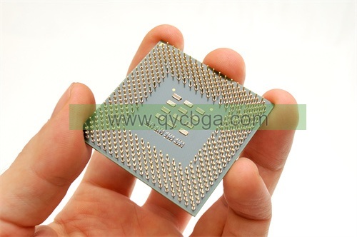
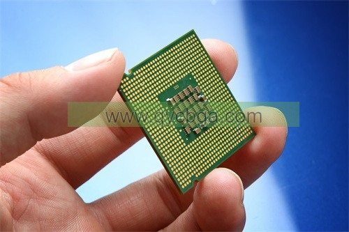
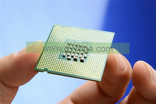
What is Wire Bonding Substrates?
Wire Bonding substrates Manufacturer,Wire bonding substrates are essential components in semiconductor packaging, providing the physical base for chip attachment and electrical connections via fine wires. These substrates are engineered to support wire bonding processes, such as gold or aluminum wire bonding, which connect the semiconductor die to the substrate’s contact pads. Key attributes include high thermal conductivity, robust mechanical strength, and excellent electrical insulation to ensure reliable performance. Typically made from materials like ceramic, organic laminates, or silicon, wire bonding substrates are chosen for their compatibility with the thermal and mechanical stresses involved in device operation. Commonly used in a range of applications from automotive to telecommunications, these substrates facilitate efficient, cost-effective manufacturing of electronic assemblies, ensuring durability and functionality in end-use environments.
Wire bonding substrates refer to the materials used as a base or foundation for wire bonding processes in semiconductor packaging. Wire bonding is a technique used in the assembly of integrated circuits (Ics) where fine wires are used to make electrical connections between a chip and the package or between different parts of the chip itself.
The substrate serves as a platform onto which the semiconductor chip is mounted, and it provides electrical connections and mechanical support for the chip. The substrate material needs to have good electrical conductivity, conductivitate termică, and mechanical properties to ensure reliable performance of the semiconductor device.
Common materials used for wire bonding substrates include:
- Ceramic substrates: Ceramică, cum ar fi alumina (Al2O3) and nitrură de aluminiu (Aln) are widely used for their excellent thermal conductivity and mechanical strength.
- Organic substrates: Materials like FR-4 (a type of fiberglass-reinforced epoxy laminate) and polyimide are used as substrates in some applications due to their lower cost and ease of processing.
- Silicon substrates: Silicon wafers can also be used as substrates for wire bonding, especially in MEMS (Micro-Electro-Mechanical Systems) applications where integration with silicon-based sensors or actuators is required.
The choice of substrate material depends on various factors including the specific requirements of the application, the operating environment, Considerații privind costurile, and manufacturing processes.

Producător de substraturi de lipire a sârmei
Wire Bonding Substrates design Reference Guide.
Designing wire bonding substrates requires careful consideration of various factors such as electrical performance, Managementul termic, mechanical stability, and manufacturability. While there isn’t a single comprehensive reference guide for wire bonding substrate design, there are several resources and guidelines available that can help engineers and designers in this process. Here are some key points to consider:
- Performanță electrică: Ensure that the substrate material has good electrical conductivity to minimize signal loss and impedance mismatch. The layout of bond pads and traces should be optimized to minimize signal distortion and crosstalk.
- Thermal Management: Choose a substrate material with high thermal conductivity to efficiently dissipate heat generated by the semiconductor device. Thermal vias and thermal pads can be incorporated into the substrate design to enhance heat dissipation.
- Mechanical Stability: The substrate should provide adequate mechanical support for the semiconductor chip and withstand mechanical stresses during handling and operation. Consider factors such as coefficient of thermal expansion (CTE) matching between the substrate and chip, as well as the mechanical strength of the substrate material.
- Package Size and Layout: Determine the size and shape of the substrate based on the requirements of the semiconductor device and the chosen packaging technology (De ex., lead-frame, flip-chip, ball grid array). Optimize the layout of bond pads, traces, and other components to minimize parasitic capacitance and inductance.
- Manufacturability: Design the substrate for ease of manufacturing and assembly. Consider factors such as the compatibility of the substrate material with standard fabrication processes, the availability of fabrication facilities, and the cost of production.
- Reliability: Ensure that the substrate design meets reliability requirements for the intended application. Perform reliability testing and analysis to identify potential failure modes such as bond wire fatigue, substrate delamination, and solder joint failure.
- Industry Standards and Guidelines: Refer to industry standards and guidelines for substrate design, such as those published by organizations like JEDEC (Joint Electron Device Engineering Council) and IPC (Association Connecting Electronics Industries).
- Simulation and Modeling: Use computer-aided design (CAD) software and simulation tools to model the electrical, termal, and mechanical behavior of the substrate design. This can help optimize the design and identify potential issues before fabrication.
By considering these factors and leveraging available resources and guidelines, engineers and designers can develop wire bonding substrate designs that meet the performance, fiabilitate, and manufacturability requirements of their semiconductor devices.
What are the materials used in Wire Bonding Substrates?
Materials used in wire bonding substrates vary depending on the specific requirements of the application, but some common materials include:
- Substraturi ceramice: Ceramică, cum ar fi alumina (Al2O3) and aluminum nitride (Aln) are widely used in high-power and high-frequency applications due to their excellent thermal conductivity, electrical insulation properties, și stabilitate mecanică.
- Organic Substrates: Organic materials such as FR-4 (a type of fiberglass-reinforced epoxy laminate), polyimide, and BT (bismaleimide triazine) resin are commonly used in low- to mid-range applications due to their lower cost, flexibility, and ease of processing.
- Silicon Substrates: Silicon wafers are used in certain applications, particularly in MEMS (Micro-Electro-Mechanical Systems) devices, where integration with silicon-based sensors or actuators is required.
- Metal Substrates: Metals such as copper, aluminum, and copper alloys are sometimes used as substrates, particularly in high-power applications where thermal conductivity is a critical consideration.
- Glass Substrates: Glass materials such as borosilicate glass are used in specialized applications where high electrical insulation and thermal stability are required.
The choice of substrate material depends on various factors including the electrical and thermal performance requirements, mechanical stability, Considerații privind costurile, and compatibility with manufacturing processes. In addition to the substrate material itself, other materials such as solder alloys, adhesives, and die attach materials are also used in the wire bonding process to create reliable electrical connections between the semiconductor chip and the substrate.
How is Wire Bonding Substrates manufactured?
Package-on-Package (POP) substrates are manufactured through a series of processes involving substrate fabrication, adunare, și ambalaje. Here’s an overview of how POP package substrates are typically manufactured:
- Fabricarea substratului:
– Selectarea materialului substratului: The first step is to select a suitable substrate material based on the requirements of the POP package, considering factors such as electrical performance, Managementul termic, și stabilitate mecanică. Common substrate materials include organic substrates (De ex., FR-4, polyimide) and ceramic substrates (De ex., Alumină, nitrură de aluminiu).
– Pregătirea substratului: The selected substrate material is prepared for fabrication by cleaning and surface treatment processes to ensure proper adhesion of subsequent layers and components.
– Lamination: For organic substrates, multiple layers of substrate material may be laminated together to create a multilayered substrate structure. This process involves applying heat and pressure to bond the layers together.
- Circuit Patterning:
– Photoresist Application: A layer of photoresist material is applied to the substrate surface.
– Exposure and Development: The substrate is exposed to UV light through a photomask, which defines the desired circuit pattern. The exposed photoresist is then developed to remove the unexposed areas, leaving behind the patterned resist.
– Gravură: The substrate is subjected to etching processes (De ex., chemical etching, plasma etching) to remove material from the exposed areas, creating the desired circuit pattern.
- Finisarea suprafeței:
– Metallization: Metal layers (typically copper) are deposited onto the substrate surface through processes such as sputtering or electroplating to form conductive traces and pads.
– Surface Treatment: Surface treatment processes such as solder mask application and surface finish (De ex., ENIG – Electroless Nickel Immersion Gold) are applied to enhance solderability and protect the circuitry.
- Component Assembly:
– Die Attach: Semiconductor chips are attached to the substrate using die attach materials such as epoxy adhesives or solder pastes.
– Lipirea sârmei: Wire bonding techniques (De ex., ball bonding, wedge bonding) are used to create electrical connections between the semiconductor chip and the substrate.
– Încapsulare: The assembled components are encapsulated with molding compounds to protect them from environmental factors such as moisture and mechanical stress.
- Testare și inspecție:
– Various electrical, mecanic, and visual inspections are conducted to ensure the quality and reliability of the POP package substrates.
- Ambalare finală:
– After passing quality control tests, the POP package substrates are packaged and labeled for distribution to customers or further assembly into electronic devices.
Throughout these manufacturing processes, stringent quality control measures are implemented to ensure that the POP package substrates meet the required specifications and standards for reliability and performance.
The Application area of Wire Bonding Substrates
Wire bonding substrates find application in various fields where integrated circuits (Ics) or semiconductor devices are used. Some common application areas of wire bonding substrates include:
- Consumer Electronics: Wire bonding substrates are extensively used in consumer electronics such as smartphones, tablets, laptops, and wearables. These substrates play a crucial role in providing electrical connections and mechanical support for semiconductor chips used in these devices.
- Automotive Electronics: In automotive electronics, wire bonding substrates are utilized in components such as engine control units (ECUs), infotainment systems, advanced driver-assistance systems (ADAS), and various sensors. They help ensure reliable performance in harsh operating conditions, including temperature variations and mechanical vibrations.
- Telecommunications: Wire bonding substrates are employed in telecommunications equipment such as routers, switches, base stations, and optical networking devices. These substrates facilitate the interconnection of semiconductor chips and support high-speed data transmission.
- Industrial Applications: Industrial equipment and machinery often incorporate wire bonding substrates in control systems, monitoring devices, robotics, and automation systems. These substrates provide the necessary electrical connectivity and durability required for industrial environments.
- Medical Devices: Wire bonding substrates play a critical role in medical devices, including diagnostic equipment, patient monitoring systems, imaging devices, and implantable medical devices. They help ensure the reliability and performance of semiconductor components used in medical applications.
- Aerospace and Defense: In aerospace and defense applications, wire bonding substrates are utilized in avionics systems, satellite communication systems, radar systems, and missile guidance systems. These substrates must meet stringent requirements for reliability, durability, and performance in extreme environments.
- Energy Systems: Wire bonding substrates are employed in energy-related applications such as power inverters, solar inverters, wind turbine controllers, and battery management systems. They provide electrical connections for semiconductor components used in energy generation, conversion, and storage systems.
- MEMS Devices: Micro-Electro-Mechanical Systems (MEMS) devices, which integrate mechanical and electrical components on a single substrate, often utilize wire bonding substrates. These devices are used in a wide range of applications, including automotive sensors, biomedical sensors, and consumer electronics.
General, wire bonding substrates are versatile components that play a crucial role in various industries, enabling the reliable operation of semiconductor devices in diverse applications. Their design and materials are tailored to meet the specific requirements of each application, ensuring optimal performance and reliability.
What are the advantages of Wire Bonding Substrates?
Wire bonding substrates offer several advantages, making them a popular choice for semiconductor packaging in various industries. Some of the key advantages include:
- Cost-Effectiveness: Wire bonding substrates are often more cost-effective compared to other packaging methods such as flip-chip bonding or wafer-level packaging. The materials used in wire bonding substrates, such as organic substrates or ceramic substrates, are generally less expensive than materials like silicon wafers used in other packaging methods.
- Flexibilitate: Wire bonding substrates are highly versatile and can accommodate a wide range of semiconductor devices, inclusiv circuite integrate (Ics), discrete components, and microelectromechanical systems (MEMS) devices. They can also support various wire bonding techniques (De ex., ball bonding, wedge bonding) and bonding materials (De ex., aluminum, gold).
- Reliability: Wire bonding technology has been widely used for decades and has a proven track record of reliability. The wire bonds formed during the assembly process provide robust electrical connections between the semiconductor device and the substrate, with good mechanical strength and thermal stability.
- Miniaturization: Wire bonding substrates allow for miniaturization of electronic devices due to their ability to accommodate small chip sizes and fine pitch bonding. This is especially important in applications such as consumer electronics, where compact form factors are desired.
- Managementul termic: Certain types of wire bonding substrates, such as ceramic substrates, offer excellent thermal conductivity, aiding in heat dissipation from the semiconductor device. This helps in maintaining optimal operating temperatures and improving the overall reliability of the device.
- Ease of Integration: Wire bonding substrates can be easily integrated into existing manufacturing processes and infrastructure, making them a convenient choice for semiconductor packaging. They can also be combined with other packaging technologies to create hybrid packages that leverage the strengths of each method.
- Compatibility with Multiple Devices: Wire bonding substrates can accommodate multiple semiconductor devices on a single substrate, allowing for the integration of diverse functionalities into a single package. This can simplify system design and reduce the overall footprint of electronic assemblies.
- Industry Standardization: Wire bonding technology is well-established and standardized in the semiconductor industry, with widely accepted guidelines and specifications for substrate design, assembly processes, and reliability testing. This ensures consistency and interoperability across different manufacturers and applications.
General, wire bonding substrates offer a compelling combination of cost-effectiveness, fiabilitate, flexibility, and ease of integration, making them a preferred choice for a wide range of semiconductor packaging applications.
How Much Does Wire Bonding Substrates Cost?
The cost of wire bonding substrates can vary widely depending on several factors such as the substrate material, size, complexity of the design, manufacturing processes involved, and quantity ordered. Here are some general considerations regarding the cost of wire bonding substrates:
- Substrate Material: Different substrate materials have different costs. For example, organic substrates (De ex., FR-4, polyimide) are generally less expensive than ceramic substrates (De ex., Alumină, nitrură de aluminiu) due to differences in material cost and manufacturing processes.
- Size and Complexity: Larger substrates or substrates with complex designs (De ex., multilayered structures, high-density interconnects) may require more material and involve additional manufacturing steps, leading to higher costs.
- Manufacturing Processes: The manufacturing processes involved in producing wire bonding substrates, such as circuit patterning, metallization, Finisarea suprafeței, and assembly, contribute to the overall cost. Processes that require specialized equipment or involve more labor-intensive steps may increase the cost.
- Volume Discounts: Typically, larger order quantities result in lower per-unit costs due to economies of scale. Manufacturers may offer volume discounts for bulk orders of wire bonding substrates.
- Customization: Customized substrate designs or specific requirements (De ex., tight tolerances, special materials, advanced features) may incur additional costs compared to standard off-the-shelf substrates.
- Supplier and Location: The choice of supplier and their location can also impact the cost of wire bonding substrates. Suppliers with lower manufacturing costs or located in regions with lower labor costs may offer more competitive pricing.
It’s important to note that the cost of wire bonding substrates is just one component of the overall cost of semiconductor packaging. Other factors such as semiconductor chip cost, assembly labor, testing, quality control, and overhead expenses also contribute to the total cost of the packaged device.
For specific pricing information, it’s best to contact substrate manufacturers or suppliers directly and request a quote based on your requirements, including substrate material, Dimensiuni, quantity, and any special considerations.
FAQs about Wire Bonding Substrates
What is a wire bonding substrate?
A wire bonding substrate is a material used as a base or foundation for wire bonding processes in semiconductor packaging. It provides electrical connections and mechanical support for semiconductor chips.
What materials are used in wire bonding substrates?
Common materials used in wire bonding substrates include ceramics (De ex., Alumină, nitrură de aluminiu), organic substrates (De ex., FR-4, polyimide), silicon, metals (De ex., copper, aluminum), and glass.
What are the advantages of wire bonding substrates?
Advantages of wire bonding substrates include cost-effectiveness, flexibility, fiabilitate, miniaturization, Managementul termic, ease of integration, compatibility with multiple devices, and industry standardization.
How much does wire bonding substrates cost?
The cost of wire bonding substrates can vary depending on factors such as substrate material, size, complexitate, Procese de fabricație, volume discounts, customization, and supplier. It’s best to contact substrate manufacturers or suppliers for specific pricing information.
What are the applications of wire bonding substrates?
Wire bonding substrates find applications in various industries where integrated circuits (Ics) or semiconductor devices are used, including consumer electronics, electronice auto, telecommunications, industrial applications, medical devices, aerospace and defense, energy systems, and MEMS devices.
How are wire bonding substrates manufactured?
Wire bonding substrates are manufactured through processes such as substrate fabrication, circuit patterning, Finisarea suprafeței, component assembly (die attach, wire bonding, encapsulation), testing and inspection, and final packaging.
What considerations are important in wire bonding substrate design?
Important considerations in wire bonding substrate design include electrical performance, Managementul termic, mechanical stability, package size and layout, manufacturability, fiabilitate, adherence to industry standards and guidelines, and simulation and modeling.
Where can I find more information about wire bonding substrates?
Additional information about wire bonding substrates can be found through technical literature, industry publications, manufacturer datasheets, and consulting with experts in semiconductor packaging.
 Producător de substrat de pachet FCBGA

