What is WLP Package Substrate?
Fabricante de substrato de pacote WLP,WLP (Wafer-Level Package) package substrate is an advanced packaging technology that allows semiconductor devices to be packaged at the wafer level, rather than individually. This method streamlines the manufacturing process, reduces costs, and enhances performance. WLP substrates provide excellent electrical performance, efficient thermal management, and robust mechanical stability. They are typically made from materials like silicon or advanced polymers and support high-density interconnections with minimal signal loss. Ideal for compact and high-performance applications, WLP is widely used in mobile devices, wearable technology, and IoT devices. This packaging solution enables significant miniaturization, ensuring reliability and efficiency in modern electronic systems.
WLP stands for Wafer Level Packaging, which is a technology used in semiconductor packaging where the IC (integrated circuit) is encapsulated at the wafer level before the individual chips are separated. WLP offers advantages in terms of size, performance, and cost compared to traditional packaging methods.
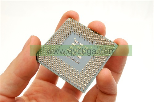
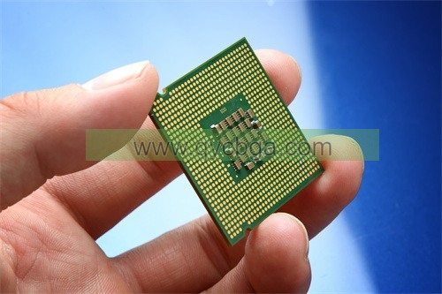
The WLP package substrate is the material that serves as the foundation for the integrated circuit and its connections within the package. It provides electrical connections between the chip and the outside world (such as PCBs or other electronic components) while also providing mechanical support and protection for the chip.
The substrate material can vary depending on the specific requirements of the application, but commonly used materials include silicon, glass, and various types of polymers. These substrates are typically very thin and are designed to optimize electrical performance while minimizing the overall package size.
Geral, the WLP package substrate is a critical component in the assembly of integrated circuits using Wafer Level Packaging technology, enabling smaller, more efficient, and more cost-effective semiconductor devices.
WLP Package Substrate design Reference Guide.
Designing a WLP (Wafer Level Packaging) package substrate requires careful consideration of various factors to ensure optimal performance, fiabilidade, and manufacturability. This reference guide aims to provide a comprehensive overview of key aspects to consider when designing WLP package substrates.
- Electrical Performance: The substrate design must facilitate efficient electrical connections between the IC and external components while minimizing signal loss and noise. Key considerations include signal routing, Correspondência de impedância, and power distribution.
- Integridade do sinal: Proper signal integrity is crucial to prevent data corruption or loss. Design techniques such as controlled impedance routing, signal length matching, and power/ground plane placement are essential to maintain signal integrity.
- Gerenciamento térmico: Efficient heat dissipation is critical to prevent overheating and ensure long-term reliability. The substrate design should incorporate features such as thermal vias, heat spreaders, and thermal pads to facilitate heat transfer away from the IC.
- Mechanical Integrity: The substrate must provide adequate mechanical support to withstand mechanical stress during handling, assembléia, and operation. Design considerations include substrate thickness, Seleção de material, and reinforcement structures.
- Package Size and Form Factor: WLP is known for its compact size, making it ideal for space-constrained applications. The substrate design should be optimized to minimize package footprint while accommodating all necessary electrical and mechanical components.
- Capacidade de fabricação: Design for manufacturability (DFM) is essential to ensure smooth and cost-effective production. Considerations include substrate fabrication techniques, alignment tolerances, and assembly processes.
- Reliability: The substrate design should meet stringent reliability requirements to ensure long-term performance in various operating conditions. Factors such as material selection, interconnect reliability, and environmental robustness should be carefully evaluated.
- Cost Optimization: Balancing performance and cost is crucial in WLP substrate design. Techniques such as substrate panelization, material optimization, and standardized assembly processes can help minimize production costs without compromising quality.
- Compliance and Standards: Ensure that the substrate design complies with relevant industry standards and regulations, such as JEDEC standards for semiconductor packaging.
- Simulation and Testing: Utilize advanced simulation tools and testing methodologies to evaluate and validate the substrate design before production. Techniques such as finite element analysis (FEA) and signal integrity simulations can help identify and address potential issues early in the design process.
By considering these key aspects and leveraging advanced design tools and methodologies, engineers can develop WLP package substrates that meet performance, fiabilidade, and cost requirements for a wide range of semiconductor applications.

Fabricante de substrato de pacote WLP
What are the materials used in WLP Package Substrate?
Wafer Level Packaging (WLP) substrates utilize various materials to provide electrical connections, mechanical support, and thermal management for integrated circuits (ICs). Some common materials used in WLP package substrates include:
- Organic Substrates: Organic substrates, typically made of epoxy-based materials, are commonly used in WLP for their cost-effectiveness and ease of processing. Examples include FR-4 (Flame Retardant 4), BT (Bismaleimide Triazine), and PI (Polyimide). Organic substrates offer good electrical properties, mechanical flexibility, and are suitable for high-volume manufacturing.
- Silicon: Silicon substrates are used in WLP for their excellent electrical properties, thermal conductivity, and compatibility with semiconductor fabrication processes. Silicon substrates can be fabricated with advanced semiconductor manufacturing techniques, allowing for integrated circuitry to be directly built on the substrate surface.
- Glass: Glass substrates offer high electrical insulation and thermal stability, making them suitable for demanding WLP applications. Glass substrates can be fabricated with fine features using techniques such as laser micromachining or chemical etching.
- Ceramics: Ceramic substrates, such as alumina (Al2O3) and aluminum nitride (AlN), are valued for their high thermal conductivity and mechanical strength. Ceramic substrates are often used in WLP for applications requiring excellent thermal management and reliability in harsh environments.
- Metal: Metal substrates, such as copper (Cu) or aluminum (Al), are used in WLP for their superior thermal conductivity and mechanical stability. Metal substrates are often employed as heat spreaders or thermal vias to enhance heat dissipation from the integrated circuit.
- Polymer Composites: Polymer composites, such as filled polymers or polymer-ceramic hybrids, offer a combination of electrical insulation, mechanical strength, and thermal performance. Polymer composites can be tailored to meet specific requirements for WLP applications, including cost-effective manufacturing and compatibility with advanced packaging techniques.
The choice of substrate material depends on various factors such as electrical performance, thermal management requirements, mechanical stability, cost considerations, and compatibility with the semiconductor fabrication process. By selecting the appropriate substrate material and optimizing the substrate design, engineers can develop WLP packages that meet the performance, fiabilidade, and cost targets for a wide range of semiconductor applications.
How is WLP Package Substrate manufactured?
The manufacturing process of Wafer Level Packaging (WLP) substrates involves several steps to create the necessary electrical connections, mechanical support, and thermal management features for integrated circuits (ICs) at the wafer level. Here is a general overview of the typical manufacturing process for WLP package substrates:
- Substrate Preparation: The manufacturing process begins with the preparation of the substrate material, which can be organic (e.g., epoxy-based), silicon, glass, ceramics, metal, or polymer composites. The substrate material is typically in the form of thin wafers or sheets.
- Surface Preparation: The substrate surface is cleaned and treated to ensure proper adhesion and compatibility with subsequent processing steps. This may involve cleaning with solvents, chemical treatments, or plasma etching.
- Layer Deposition: Various layers are deposited onto the substrate surface to create the necessary features for electrical interconnections, such as metal traces, dielectric layers, and barrier films. Techniques such as physical vapor deposition (PVD), chemical vapor deposition (CVD), sputtering, or plating are used to deposit these layers.
- Patterning: Photolithography and etching processes are used to define the desired patterns for electrical interconnects, vias, and other features on the substrate surface. Photomasks containing the desired patterns are used to transfer the patterns onto the substrate through exposure to UV light and chemical etching.
- Metallization: Metal layers are deposited onto the substrate surface to create conductive traces and vias for electrical connections. Techniques such as electroplating, sputtering, or chemical vapor deposition (CVD) are used to deposit the metal layers.
- Die Attach and Wire Bonding (optional): In some cases, integrated circuits (ICs) are attached directly onto the substrate surface using die attach materials, and wire bonding techniques are used to make electrical connections between the IC and the substrate.
- Encapsulation: The substrate and attached ICs are encapsulated with a protective layer of epoxy resin or other encapsulant materials to provide mechanical support and environmental protection. This encapsulation process may involve molding, dispensing, or underfilling techniques.
- Thermal Management Features: Additional thermal management features such as heat spreaders, thermal vias, or thermal interface materials may be incorporated into the substrate design to enhance heat dissipation from the ICs.
- Testing and Inspection: The manufactured WLP substrates undergo rigorous testing and inspection processes to ensure electrical functionality, mechanical integrity, and compliance with quality standards.
- Packaging and Assembly: After testing and inspection, the WLP substrates are ready for integration into final semiconductor packages. They may be assembled onto printed circuit boards (PCBs) or other electronic assemblies using surface mount technology (SMT) or other packaging techniques.
Geral, the manufacturing process of WLP package substrates involves a combination of material deposition, patterning, metallization, encapsulation, and testing steps to create high-performance and reliable substrates for semiconductor packaging applications.
The Application area of WLP Package Substrate
Wafer Level Packaging (WLP) package substrates find application across various industries and technologies where compact, high-performance, and cost-effective semiconductor packaging solutions are required. Some of the key application areas of WLP package substrates include:
- Mobile Devices: WLP is widely used in smartphones, tablets, wearables, and other mobile devices due to its compact size and ability to accommodate multiple chips in a small footprint. WLP substrates enable the miniaturization of electronic components, allowing manufacturers to produce thinner and lighter mobile devices with improved performance.
- Consumer Electronics: Beyond mobile devices, WLP substrates are also utilized in a range of consumer electronics products such as digital cameras, gaming consoles, smart TVs, and audio devices. The compact size and high-density interconnects offered by WLP enable manufacturers to design sleeker and more feature-rich consumer electronics products.
- Automotive Electronics: WLP is increasingly being adopted in automotive electronics applications for its ability to withstand harsh environmental conditions, vibration, and temperature extremes. WLP substrates are used in advanced driver assistance systems (ADAS), infotainment systems, engine control units (ECUs), and other automotive electronics to improve performance, fiabilidade, and durability.
- Internet of Things (IoT) Devices: IoT devices, including sensors, actuators, and connected appliances, often require compact and energy-efficient semiconductor packaging solutions. WLP substrates enable the integration of complex electronic components into small IoT devices, enabling connectivity, sensing, and data processing capabilities.
- Medical Devices: In medical device applications, where space constraints and reliability are critical considerations, WLP substrates offer advantages in terms of size, performance, e confiabilidade. WLP is used in medical imaging devices, patient monitoring systems, implantable devices, and diagnostic equipment to enable compact and reliable electronics solutions for healthcare applications.
- Industrial and Aerospace: WLP substrates are utilized in industrial automation, aerospace, and defense applications where ruggedness, fiabilidade, and performance are paramount. WLP enables the integration of sophisticated electronics into industrial machinery, aerospace systems, and defense equipment, enabling advanced functionality and mission-critical operations.
- Networking and Telecommunications: WLP substrates play a crucial role in networking and telecommunications equipment, including routers, switches, base stations, and optical transceivers. WLP enables high-speed data processing, efficient power management, and compact form factors for telecommunications infrastructure and networking devices.
- High-Performance Computing (HPC): In high-performance computing applications such as data centers, supercomputers, and cloud computing servers, WLP substrates are used to package high-speed processors, memory modules, and other critical components. WLP enables dense integration, high-speed interconnectivity, and efficient thermal management in HPC systems.
Geral, the versatility, compactness, and performance of WLP package substrates make them well-suited for a wide range of applications across industries, driving innovation and enabling the development of advanced electronic products and systems.
What are the advantages of WLP Package Substrate?
Wafer Level Packaging (WLP) package substrates offer several advantages compared to traditional packaging methods, making them a preferred choice for many semiconductor applications. Some of the key advantages of WLP package substrates include:
- Miniaturization: WLP enables the packaging of integrated circuits (ICs) directly at the wafer level, eliminating the need for additional packaging materials such as lead frames or ceramic packages. This results in significantly smaller and thinner packages, enabling manufacturers to create more compact and lightweight electronic devices.
- Improved Electrical Performance: WLP package substrates offer shorter electrical interconnect lengths compared to traditional packaging methods, leading to reduced parasitic capacitance and inductance. This results in improved electrical performance, including higher speed, lower power consumption, and better signal integrity.
- Higher Integration Density: WLP allows for the integration of multiple ICs, passive components, and interconnects within a single package, enabling higher integration density and functionality. This is particularly advantageous for applications requiring complex system-on-chip (SoC) designs or multi-chip modules (MCMs).
- Enhanced Thermal Management: WLP package substrates facilitate efficient heat dissipation from the ICs due to their compact size and direct attachment to the substrate material. This enables better thermal management, reduces hot spots, and improves overall reliability and performance of the semiconductor devices.
- Cost Efficiency: WLP eliminates the need for additional packaging materials, assembly steps, and testing processes associated with traditional packaging methods, leading to lower manufacturing costs. Adicionalmente, WLP enables higher yields and throughput in semiconductor fabrication, further contributing to cost efficiency.
- Improved Mechanical Stability: WLP package substrates provide robust mechanical support to the ICs due to their direct attachment to the substrate material. This enhances the mechanical stability and reliability of the semiconductor devices, particularly in applications subject to mechanical stress or vibration.
- Simplified Assembly Processes: WLP streamlines the assembly process by integrating packaging and interconnects at the wafer level, reducing the number of assembly steps and associated equipment requirements. This simplification of the assembly process results in faster time-to-market and increased manufacturing efficiency.
- Compatibility with Advanced Technologies: WLP package substrates are compatible with advanced semiconductor manufacturing technologies, including flip-chip bonding, through-silicon vias (TSVs), and micro-electromechanical systems (MEMS). This enables the integration of advanced features and functionalities into semiconductor devices.
Geral, the advantages of WLP package substrates, including miniaturization, improved electrical performance, higher integration density, enhanced thermal management, cost efficiency, mechanical stability, simplified assembly processes, and compatibility with advanced technologies, make them an attractive choice for a wide range of semiconductor applications.
How Much Does WLP Package Substrate Cost?
The cost of Wafer Level Packaging (WLP) package substrates can vary significantly depending on several factors, including the substrate material, design complexity, manufacturing processes, volume production, and supplier/vendor pricing. Contudo, here are some general factors that can influence the cost of WLP package substrates:
- Substrate Material: Different substrate materials, such as organic (e.g., epoxy-based), silicon, glass, ceramics, metal, or polymer composites, have varying costs associated with their fabrication and processing. For example, silicon and ceramic substrates tend to be more expensive compared to organic substrates.
- Design Complexity: The complexity of the substrate design, incluindo o número de camadas, the density of interconnects, and the inclusion of advanced features such as thermal management structures or through-silicon vias (TSVs), can impact manufacturing costs. More complex designs typically require additional processing steps and higher precision, leading to higher costs.
- Manufacturing Processes: The choice of manufacturing processes, such as deposition techniques, photolithography, etching, metallization, encapsulation, and testing, can influence the overall cost of producing WLP package substrates. Advanced manufacturing processes may require specialized equipment and expertise, adding to the manufacturing cost.
- Volume Production: Economies of scale play a significant role in determining the cost of WLP package substrates. Higher volume production typically leads to lower per-unit costs due to spreading fixed costs across a larger number of units. Conversely, low-volume production may incur higher costs per unit due to lower efficiency and utilization of manufacturing facilities.
- Supplier/Vendor Pricing: The pricing policies of substrate suppliers/vendors can vary based on factors such as material sourcing, manufacturing capabilities, technological expertise, and market competition. Prices may also be influenced by contractual agreements, negotiation strategies, and fluctuations in raw material costs.
- Quality and Reliability Requirements: Meeting stringent quality and reliability requirements, such as industry standards, reliability testing, and customer specifications, may entail additional costs associated with quality assurance measures, testing procedures, and compliance certifications.
Geral, the cost of WLP package substrates can range from a few cents to several dollars per unit, depending on the specific requirements of the application and the factors mentioned above. It’s essential for manufacturers to carefully evaluate these factors and work closely with suppliers/vendors to optimize costs while meeting performance, fiabilidade, and quality objectives.
Perguntas frequentes
What is Wafer Level Packaging (WLP) and how does it differ from traditional packaging methods?
Wafer Level Packaging (WLP) is a semiconductor packaging technology where the integrated circuits (ICs) are encapsulated directly at the wafer level before they are separated into individual chips. This differs from traditional packaging methods, such as chip-on-board (COB) or flip-chip packaging, where packaging is performed after the chips have been separated.
What are the advantages of using WLP package substrates?
WLP package substrates offer advantages such as miniaturization, improved electrical performance, higher integration density, enhanced thermal management, cost efficiency, simplified assembly processes, and compatibility with advanced technologies.
What materials are commonly used in WLP package substrates?
Common materials used in WLP package substrates include organic substrates (e.g., epoxy-based), silicon, glass, ceramics, metal, and polymer composites. The choice of material depends on factors such as electrical performance, thermal management requirements, mechanical stability, and cost considerations.
How is a WLP package substrate manufactured?
The manufacturing process of WLP package substrates involves steps such as substrate preparation, surface preparation, layer deposition, patterning, metallization, encapsulation, thermal management feature incorporation, teste, and inspection. Advanced semiconductor manufacturing techniques such as photolithography, etching, deposition, and assembly processes are employed to create high-performance and reliable substrates.
What are the application areas of WLP package substrates?
WLP package substrates find application across various industries and technologies, including mobile devices, consumer electronics, Eletrônica automotiva, Internet of Things (IoT) devices, medical devices, industrial and aerospace applications, networking and telecommunications equipment, e computação de alto desempenho (HPC) systems.
What factors influence the cost of WLP package substrates?
The cost of WLP package substrates can vary depending on factors such as substrate material, design complexity, manufacturing processes, volume production, and supplier/vendor pricing. Economies of scale, quality and reliability requirements, and technological advancements also influence the overall cost.
What are some key considerations when designing WLP package substrates?
Key considerations when designing WLP package substrates include electrical performance, Integridade do sinal, Gerenciamento térmico, mechanical integrity, package size and form factor, manufacturability, fiabilidade, compliance with standards, simulation and testing, and cost optimization.
 Fabricante de substrato de pacote FCBGA

