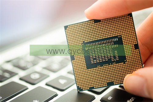
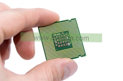
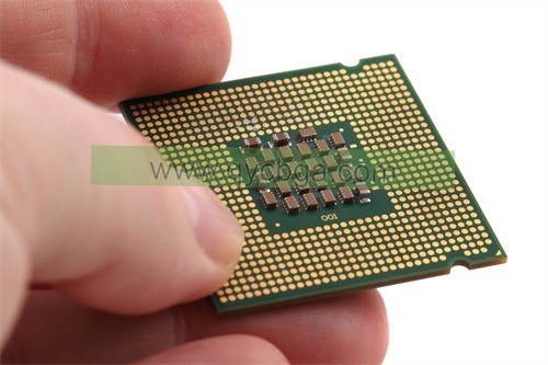
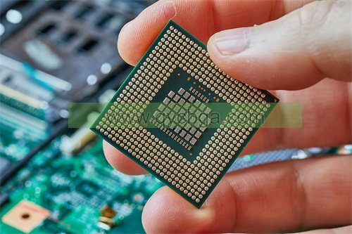
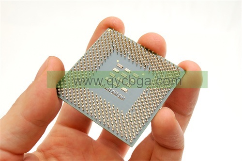
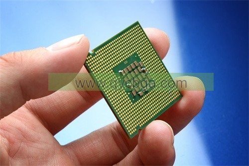
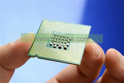
What is BT Package Substrate?
BT Package Substrate Manufacturer.BT (Bismaleimide Triazine) package substrate is a high-performance material widely used in semiconductor packaging. Known for its excellent electrical insulation properties and high thermal stability, BT substrate provides reliable performance for integrated circuits. It features a low coefficient of thermal expansion, matching well with silicon, which reduces stress and enhances durability. This substrate also offers superior mechanical strength and moisture resistance, making it ideal for use in harsh environments. Commonly employed in applications such as mobile devices, computers, and automotive electronics, BT package substrates ensure robust and efficient performance in compact and high-density electronic assemblies.
BT Package Substrate is utilized in the assembly and packaging of semiconductor devices, particularly in flip-chip packaging and multi-chip module applications. It provides mechanical support, electrical connectivity, and thermal dissipation for the integrated circuits (ICs) mounted on it.
BT Package Substrate offers several advantages, including high thermal conductivity, excellent dimensional stability, and good electrical properties. These characteristics make it suitable for applications where heat dissipation and electrical performance are critical, such as in high-performance computing, networking, and telecommunications equipment.
Geral, BT Package Substrate plays a crucial role in ensuring the reliability and performance of semiconductor devices by providing a robust platform for mounting and interconnecting integrated circuits.

Fabricante de substrato de pacote BT
BT Package Substrate Design Reference Guide.
“BT Package Substrate Design Reference Guide” is a reference guide for BT package substrate design. This guide may contain detailed information on how to design and utilize BT package substrates, as well as content regarding best practices, design principles, and recommendations.
Such a guide typically provides guidance for engineers and designers on how to effectively incorporate BT package substrates into their electronic products. It may cover various topics, including substrate layout, package material selection, electrical and thermal characteristics, interlayer connections, protective design, and more.
By referring to such a guide, engineers can better understand how to leverage the advantages of BT package substrates and follow best practices to design high-performance, reliable, and cost-effective electronic products.
What are the materials used in BT Package Substrate?
BT Package Substrates typically consist of several materials that are carefully selected to meet the requirements of high-performance semiconductor packaging. The primary materials used in BT Package Substrates include:
- 1. Bismaleimide Triazine (BT) Resin: This is the main material in BT Package Substrates, providing mechanical support and electrical insulation. BT resin offers excellent thermal stability, low coefficient of thermal expansion (CTE), and high-temperature resistance, making it ideal for applications where thermal management is crucial.
- Copper (Cu) Foil: Copper foil is often used as the conductive layer in BT Package Substrates. It provides electrical connectivity for the integrated circuits (ICs) mounted on the substrate.
- Dielectric Materials: Various dielectric materials are incorporated into BT Package Substrates to provide insulation between conductive layers and to manage signal integrity. These materials may include epoxy-based resins, glass fiber reinforced materials, or other low-loss dielectrics.
- Solder Mask: Solder mask is applied to the surface of the substrate to define the areas where solder connections will be made and to protect the underlying layers from environmental factors.
- Acabamento de superfície: Surface finishes such as electroless nickel immersion gold (ENIG), organic solderability preservatives (OSP), or immersion tin may be applied to the substrate to enhance solderability and prevent oxidation of copper traces.
These materials are carefully selected and engineered to ensure the reliability, Desempenho térmico, and electrical characteristics required for advanced semiconductor packaging applications using BT Package Substrates.
How is BT Package Substrate manufactured?
The manufacturing process of BT Package Substrates involves several steps, each aimed at creating a substrate that meets the required specifications for use in semiconductor packaging. While specific manufacturing methods may vary depending on factors such as the desired substrate design and technology node, the following are common steps involved in the fabrication of BT Package Substrates:
- Substrate Preparation: The process begins with preparing the base material, typically bismaleimida triazina (BT) resin, in the form of sheets or panels. These substrates are usually pre-treated to ensure uniformity and cleanliness before further processing.
- Lamination: Layers of copper foil and dielectric materials are laminated onto the substrate material using heat and pressure. Copper foil is often used as the conductive layer, while dielectric materials provide insulation between conductive layers and manage signal integrity. The lamination process may involve multiple steps to build up the desired number of copper and dielectric layers.
- Padronização de Circuito: A photoresist layer is applied to the surface of the substrate, followed by exposure to ultraviolet light through a photomask containing the desired circuit pattern. After exposure, the substrate is developed to remove the unexposed photoresist, leaving behind the patterned areas where copper traces will be formed.
- Copper Etching: The exposed copper areas are etched away using chemical etchants, leaving behind the desired copper circuitry pattern on the substrate surface. The remaining photoresist is then stripped to reveal the patterned copper traces.
- Surface Finishing: Surface finishes such as electroless nickel immersion gold (ENIG), organic solderability preservatives (OSP), or immersion tin are applied to the substrate surface to enhance solderability and prevent oxidation of copper traces.
- Drilling and Plating: Holes for through-hole vias or microvias are drilled into the substrate, followed by a plating process to metallize the hole walls and create electrical connections between different layers of the substrate.
- Aplicação de máscara de solda: A solder mask layer is applied over the substrate surface, leaving openings for solder connections at specific locations. The solder mask helps define the areas for soldering and protects the underlying layers from environmental factors.
- Inspeção Final e Testes: The finished BT Package Substrates undergo thorough inspection and testing to ensure they meet the required specifications for dimensional accuracy, electrical connectivity, e confiabilidade.
Geral, the manufacturing process of BT Package Substrates involves a combination of material preparation, layer lamination, Padronização de circuitos, surface treatment, and finishing processes to create substrates suitable for advanced semiconductor packaging applications.
The Application area of BT Package Substrate.
BT Package Substrates find application in various areas within the semiconductor industry and electronic manufacturing sector. Some of the primary application areas include:
- High-Performance Computing (HPC): BT Package Substrates are utilized in the assembly of high-performance computing systems, including servers, supercomputers, and data centers. These substrates offer efficient thermal management and reliable electrical connectivity, critical for the demanding requirements of HPC applications.
- Networking Equipment: In networking infrastructure such as routers, switches, and telecommunications equipment, BT Package Substrates are used for their ability to handle high-speed data transmission while maintaining signal integrity and thermal stability.
- Consumer Electronics: BT Package Substrates are integrated into various consumer electronic devices, including smartphones, tablets, and gaming consoles, where compact form factors, high performance, and reliability are essential.
- Automotive Electronics: With the increasing integration of electronic systems in modern vehicles, BT Package Substrates are employed in automotive applications for functions such as engine control units (ECUs), infotainment systems, advanced driver-assistance systems (ADAS), and electric vehicle powertrains.
- Industrial and Aerospace Applications: BT Package Substrates are used in industrial automation systems, aerospace electronics, and defense applications where ruggedness, fiabilidade, and resistance to harsh environmental conditions are critical.
- Medical Devices: In medical equipment and devices, BT Package Substrates are employed for their ability to provide precise electrical connections and thermal management, supporting the functionality and reliability of medical diagnostic and imaging systems, patient monitoring devices, and implantable medical devices.
- Data Storage: BT Package Substrates play a role in data storage devices such as solid-state drives (SSDs) and hard disk drives (HDDs), where they contribute to the overall performance and reliability of the storage systems.
Geral, BT Package Substrates are versatile components used across a wide range of applications in electronics manufacturing, enabling the development of high-performance, reliable, and compact electronic devices across various industries.
What are the advantages of BT Package Substrate?
BT (Bismaleimide Triazine) Package Substrates offer several advantages over traditional substrates, making them a preferred choice for various semiconductor packaging applications. Some of the key advantages include:
- High Thermal Conductivity: BT Package Substrates exhibit excellent thermal conductivity, allowing efficient dissipation of heat generated by integrated circuits (ICs). This property helps in maintaining optimal operating temperatures, which is crucial for the reliability and performance of semiconductor devices, especially in high-power applications.
- Low Coefficient of Thermal Expansion (CTE): BT Package Substrates have a relatively low CTE, meaning they undergo minimal dimensional changes with temperature fluctuations. This characteristic helps in reducing mechanical stress on the mounted components, preventing solder joint failures and ensuring long-term reliability.
- High-Temperature Resistance: BT substrates can withstand elevated temperatures encountered during assembly processes such as solder reflow and during device operation. This high-temperature resistance ensures the integrity of the substrate and prevents deformation or degradation of electrical properties under harsh conditions.
- Excellent Electrical Properties: BT Package Substrates offer good electrical insulation properties and low signal loss, enabling reliable signal transmission and minimizing signal distortion. This is particularly important for high-frequency applications such as telecommunications and data communication.
- Dimensional Stability: BT substrates maintain dimensional stability even under thermal stress, ensuring precise alignment of components and consistent performance over time. This stability is critical for the reliability and functionality of semiconductor devices, especially in miniaturized and densely packed electronic systems.
- Compatibility with Advanced Packaging Technologies: BT Package Substrates are compatible with various advanced packaging techniques such as flip-chip, chip-on-board (COB), and system-in-package (SiP) assembléia. This compatibility allows for the integration of multiple components in a compact form factor, enhancing device functionality and performance.
- Environmental Friendliness: BT substrates are often considered environmentally friendly compared to some other substrate materials due to their halogen-free composition and lower environmental impact during manufacturing processes.
Geral, the advantages of BT Package Substrates, including their thermal properties, electrical performance, dimensional stability, and compatibility with advanced packaging technologies, make them an attractive choice for applications requiring high reliability, performance, and thermal management capabilities.
How Much Does BT Package Substrate Cost?
The cost of BT Package Substrates can vary significantly depending on various factors such as the substrate size, complexity of the design, materials used, manufacturing processes, supplier pricing, and market demand. Generally, BT Package Substrates are considered to be more expensive compared to conventional substrates due to their advanced materials and manufacturing techniques.
It’s challenging to provide a precise cost without specific details about the requirements of the substrate and the quantities involved. Adicionalmente, pricing information is often proprietary and subject to negotiation between buyers and suppliers.
Contudo, as a rough estimate, BT Package Substrates can range from a few dollars to tens or even hundreds of dollars per unit, depending on the factors mentioned above. Large-scale production runs may result in lower per-unit costs due to economies of scale, while custom or low-volume orders may incur higher costs.
For accurate pricing information, it’s recommended to consult with substrate manufacturers or suppliers directly, providing them with detailed specifications and quantities required for a more precise quotation.
FAQ
What is BT Package Substrate?
BT Package Substrate refers to a type of packaging substrate used in the semiconductor industry. It typically consists of materials such as bismaleimide triazine (BT) resin, folha de cobre, dielectric materials, solder mask, and surface finishes.
Where are BT Package Substrates used?
BT Package Substrates find application in various areas within the semiconductor industry and electronic manufacturing sector, including high-performance computing, networking equipment, consumer electronics, Eletrônica automotiva, industrial applications, medical devices, and data storage.
How are BT Package Substrates manufactured?
The manufacturing process for BT Package Substrates typically involves several steps, including substrate material preparation, layer buildup using sequential lamination, circuit formation through processes such as etching and plating, acabamento superficial, aplicação de máscara de solda, and final testing and inspection.
What factors affect the cost of BT Package Substrate?
The cost of BT Package Substrates can vary depending on factors such as substrate size, complexity of design, materials used, manufacturing processes, supplier pricing, and market demand. Larger quantities and economies of scale may lead to lower per-unit costs.
Where can I obtain BT Package Substrates?
BT Package Substrates are typically supplied by semiconductor packaging substrate manufacturers or suppliers. They can be sourced directly from manufacturers or through distributors specializing in electronic components.
Are there different types of BT Package Substrates?
Yes, there are various types of BT Package Substrates designed to meet specific application requirements. These may include different substrate materials, layer configurations, surface finishes, and thermal management solutions tailored to the needs of different industries and applications.
What considerations should be made when selecting BT Package Substrates?
When selecting BT Package Substrates, factors such as thermal performance, Propriedades elétricas, dimensional stability, fiabilidade, cost, and compatibility with assembly processes should be carefully evaluated to ensure optimal performance and cost-effectiveness for the intended application.
 Fabricante de substrato de pacote FCBGA

