Sobre Contato |

GLOBAL FLIP CHIP PACKAGE SUBSTRATE

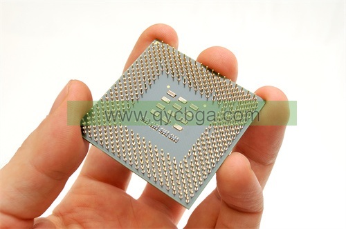
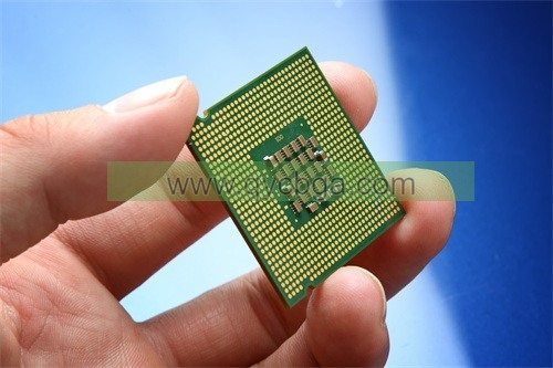
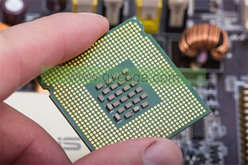
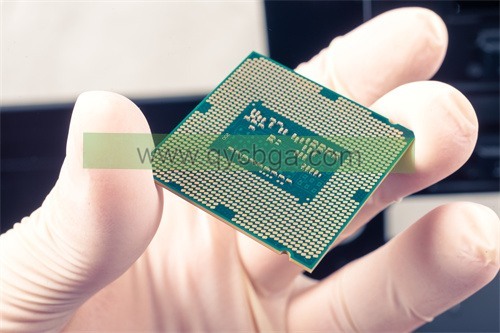
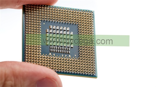
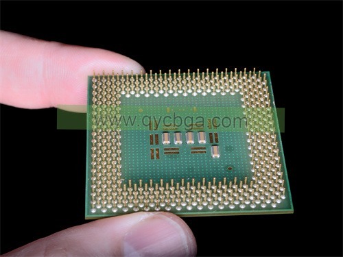
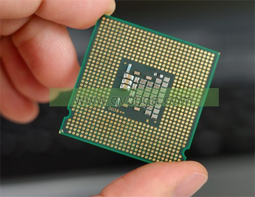
In the ever-evolving realm of electronics manufacturing, precision and reliability are paramount. SHENZHEN QYC CO., LTD is a professional producer of Flip Chip Package Substrates, boasting over 10,000 dedicated employees and state-of-the-art equipment sourced exclusively from Japan. We take pride in consistently delivering top-quality FC BGA substrates, with quality assurance serving as the cornerstone of our operations. The high-precision equipment we meticulously select from Japan forms the backbone of our commitment to providing best-in-class FC BGA substrates, resulting in a level of quality and stability that our customers can unequivocally trust.

Our production capabilities span a wide range of designs, from 4 Para 20 layers of Flip Chip Package Substrates. Whether your project necessitates a compact design or a multi-layer solution, our expertise and infrastructure are tailored to meet your requirements. What sets us apart is our ability to work with exceptional precision, boasting a minimum line width and pitch of 9 micrometers each. Our production turnaround time typically ranges from 1 Para 2 Meses. Despite our rapid production pace, quality remains our primary focus. We firmly believe that quality cannot be compromised, even when faced with tight schedules. Thus, each project undergoes rigorous quality control and testing procedures to ensure that every Package Substrate produced exhibits exceptional performance and reliability. This swift delivery is seamlessly combined with an unwavering commitment to upholding the highest quality standards, ensuring a smooth and seamless progression of your project.

Material selection is crucial in the Package Substrate manufacturing process. We offer a wide variety of packaging substrate materials, with the majority sourced from Asia, including Japan, South Korea, Taiwan, and China. Recognizing the uniqueness of each project, we remain flexible in selecting and utilizing the most suitable materials based on our customers' needs, ensuring that the Package Substrates produced perfectly align with the specific requirements of the project.

Our goal is to provide excellent solutions, drive continuous development in the electronics industry, and create greater value for our customers. We eagerly anticipate the opportunity to collaborate with you and collectively achieve project success.

Why Choose Us

We are a company specializing in the production of small pitch, high multilayer (up to 20 layers) semiconductor packaging substrates and ultra-thin HDI circuit boards with the smallest trace/spacings. Our product listings are presented in article format, emphasizing product features rather than production data, for optimal visibility in Google network promotions. Clients can reach out to us anytime for inquiries regarding the design or production of packaging substrates and HDI PCBs, and our engineers will promptly respond.

The types of packaging substrates we offer include BT, ceramic, cavity, rigid-flex, semiconductor, FCCSP, SIP, WLP, POP, wire bonding, SOP, PBGA, BGA/IC, LCC, DIP, FCBGA, ABF (Ajinomoto), MIS, microtrace, 3D IC, glass, and more.

Moreover, we operate several advanced packaging production lines, providing professional packaging services. Our team consists of over 200 engineers dedicated to resolving technical and design challenges. Should there be any doubts about production capabilities during the packaging substrate design process, or uncertainty about the factory's ability to produce satisfactory substrates according to design requirements, feel free to contact us.


Every month, we welcome 100 Para 200 new customers from around the world, some discovering us through online channels while others are referred by existing clients. With our extensive international collaboration experience, we are equipped to handle various needs and challenges. Our quality remains stable and reliable, with advanced equipment and the use of high-quality materials specified by clients.

Our goal is to ensure that every customer receives top-notch service and products. Through active collaboration, we aim to drive project success and achieve excellence in packaging substrate design and manufacturing. Regardless of the complexity of challenges, we are committed to working with clients to create outstanding solutions and achieve project goals. We look forward to establishing close working relationships with clients and providing them with professional support and advice.

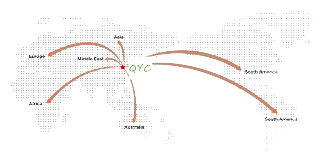
Sales Network

What sets us apart from the competition? Our ability to listen to our customers!

Our goal of achieving 100% customer satisfaction has transformed us from a single-product company into a progressive enterprise. We now offer world-class, high-quality FC-BGA (Flip Chip Ball Grid Array) boards widely used across various industries such as servers, artificial intelligence, networking, communications, military, industrial, aerospace, and more. Our technology and products span multiple critical areas, providing support to different sectors in meeting the modern electronic devices' demands for high density, high performance, and high reliability.

Every month, we welcome approximately 100 Para 200 new customers from around the world. Some discover us through online channels, while others are referred by our existing customers. Our customer base extends across several countries, reflecting the international impact and recognition of our products and services.

Send Your Inquiry


    Deixe um recado