
Microtrace Package Substrate Manufacturer
Microtrace Package Substrate Manufacturer,Microtrace Package Substrates are integral components in the realm of microelectronics packaging, serving as the foundational base for mounting and interconnecting electronic components with precision and efficiency. Characterized by their intricate design and fine traces, these substrates enable high-density integration of components, facilitating the miniaturization and performance enhancement of electronic devices. Their advanced construction materials, including organic laminates, 도예, and metal-core substrates, offer distinct advantages such as improved signal integrity, 효율적인 열 관리, and mechanical reliability. Employed across diverse industries ranging from consumer electronics to automotive and aerospace sectors, Microtrace Package Substrates play a pivotal role in enabling the development of compact and high-performance electronic systems. With rigorous quality control measures and adherence to industry standards, these substrates ensure optimal performance and reliability, meeting the evolving demands of modern microelectronics applications.
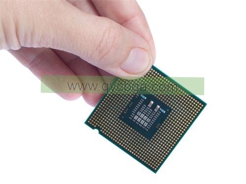
What is a Microtrace Package Substrate?
A Microtrace Package Substrate refers to a substrate material used in microelectronics packaging. In microelectronics, packaging refers to the process of enclosing integrated circuits and other electronic components in protective cases or packages. These packages provide physical protection, electrical connections, and thermal management for the enclosed components.
A microtrace package substrate typically refers to a substrate material that is specifically designed to accommodate very fine traces (conductors) and features used in modern microelectronics. These substrates are crucial components in advanced packaging technologies such as flip-chip, ball grid array (증권사), and chip-scale packaging (CSP).
The substrate material is chosen based on various factors including electrical properties, 열전도율, 열팽창 계수 (증권 시세 표시기), 기계적 강도, 및 비용. Common materials used for microtrace package substrates include various types of laminates, 도예, and metals, each with its own set of advantages and limitations.
Microtrace Package Substrate Manufacturer
What are the Microtrace Package Substrate Design Guidelines?
Microtrace package substrate design guidelines encompass a set of principles and best practices aimed at optimizing the design and performance of substrates used in microelectronics packaging, particularly those with fine traces and features. These guidelines typically include considerations related to electrical performance, 열 관리, mechanical reliability, 제조 가능성, 및 비용. Here are some key aspects often covered in such guidelines:
- Trace and Space Design: Guidelines for designing the width of traces and the spacing between them to ensure proper signal integrity, 임피던스 제어, 및 제조 가능성. This includes considerations for signal speed, 누화, and routing density.
- 비아 디자인: 비아 배치에 대한 권장 사항, 크기, and aspect ratio to facilitate interconnection between layers while minimizing signal distortion and manufacturing defects.
- Dielectric Material Selection: Guidance on selecting appropriate dielectric materials with desirable electrical properties (dielectric constant, loss tangent) and mechanical properties (증권 시세 표시기, modulus) to meet performance requirements and reliability standards.
- 열 관리: Strategies for managing heat dissipation within the package, including the use of thermal vias, 써멀 패드, and heat spreaders to minimize junction temperatures and ensure device reliability.
- Signal Integrity and Power Integrity: Techniques for optimizing signal and power integrity, such as controlled impedance routing, 디커플링 커패시터 배치, and power distribution network design to mitigate noise, voltage droops, and other electrical issues.
- Package Size and Form Factor: Considerations for optimizing the package size and form factor to meet space constraints, assembly requirements, and end-user specifications while balancing thermal and electrical performance.
- Manufacturability and Yield: Guidelines for designing substrates that are manufacturable with high yield rates, including recommendations for panelization, fiducial placement, solder mask definition, and alignment tolerances.
- 신뢰성과 내구성: Recommendations for enhancing the mechanical reliability and durability of the package substrate through design features such as controlled impedance structures, reinforcement structures, and proper material selection.
- Cost Optimization: Strategies for minimizing manufacturing costs while maintaining performance and reliability requirements, such as material selection, design simplification, and process optimization.
- Compliance and Standards: Adherence to industry standards and compliance requirements related to microelectronics packaging, such as IPC (Association Connecting Electronics Industries) standards and regulatory directives.
These guidelines may vary depending on the specific application, technology node, and packaging requirements but serve as a foundation for designing high-performance and reliable microtrace package substrates.
What is the Microtrace Package Substrate Fabrication Process?
The fabrication process of microtrace package substrates involves several steps aimed at creating the necessary substrate structure with fine traces and features for use in microelectronics packaging. While specific details may vary depending on the substrate material and manufacturing technology, the general process typically includes the following key steps:
- 기판 재료 선택: Choose a substrate material that meets the requirements of the intended application in terms of electrical, thermal, and mechanical properties. Common substrate materials include laminates (예), 프렌-4, 구체의), 도예, and metal-core substrates.
- Panel Preparation:Prepare the substrate material in the form of panels or sheets of appropriate size and thickness for subsequent processing. 여기에는 절단이 포함될 수 있습니다, cleaning, and surface treatment of the panels to ensure proper adhesion and uniformity.
- 레이어 스택업 설계: Determine the layer stackup configuration based on the desired number of signal, 힘, 및 지상 레이어. Design the layout of each layer, including the placement of traces, vias, and component pads, using computer-aided design (CAD) software.
- 박판:For multilayer substrates, assemble the individual layers into a single panel using a lamination process. This involves bonding the layers together under heat and pressure to form a solid composite structure.
- 드릴링: Drill holes or vias through the substrate panel at locations specified by the design layout. These vias are used for interconnecting different layers and components within the package.
- Through-hole Plating:Coat the walls of drilled vias with conductive material (예), copper) through a process called through-hole plating. This ensures electrical continuity between adjacent layers and facilitates soldering of components.
- Conductor Patterning: Apply a thin layer of conductive material (typically copper) onto the surface of the substrate panel using techniques such as additive (전기 도금) or subtractive (에칭) processes. Define the desired trace patterns and features using photolithography and etching techniques.
- Dielectric Layer Formation: Deposit dielectric material (예), epoxy resin) onto the substrate surface to insulate the conductive traces and provide mechanical support. This dielectric layer may be applied using techniques such as spin coating, screen printing, or lamination.
- 표면 마무리: Apply surface finishes to the substrate to improve solderability, corrosion resistance, and wire bonding capabilities. Common surface finishes include solder mask, solder plating (예), hot air leveling, electroless nickel immersion gold), and protective coatings.
- Final Inspection and Testing: Perform visual inspection, dimensional measurements, and electrical testing to ensure that the fabricated substrates meet the required specifications and quality standards.
By following these steps, manufacturers can produce microtrace package substrates with precise geometries, excellent electrical performance, and mechanical reliability for use in advanced microelectronics packaging applications.
How do you manufacture a Microtrace Package Substrate?
Manufacturing a microtrace package substrate involves several intricate processes aimed at creating a substrate with fine traces and features for use in microelectronics packaging. Here’s a step-by-step overview of the typical manufacturing process:
- 기판 재료 선택: Choose a suitable substrate material based on the specific requirements of the application, considering factors such as electrical properties, 열전도율, 기계적 강도, 및 비용. Common substrate materials include laminates (예), 프렌-4, 구체의), 도예, and metal-core substrates.
- Panel Preparation:Prepare the substrate material in the form of panels or sheets of appropriate size and thickness for subsequent processing. 여기에는 절단이 포함될 수 있습니다, cleaning, and surface treatment of the panels to ensure proper adhesion and uniformity.
- 레이어 스택업 설계: Design the layer stackup configuration based on the desired number of signal, 힘, 및 지상 레이어. Use computer-aided design (CAD) software to layout each layer, including the placement of traces, vias, and component pads.
- 박판: For multilayer substrates, assemble the individual layers into a single panel using a lamination process. This typically involves bonding the layers together under heat and pressure to form a solid composite structure.
- 드릴링: Drill holes or vias through the substrate panel at locations specified by the design layout. These vias are used for interconnecting different layers and components within the package.
- Through-hole Plating: Coat the walls of drilled vias with conductive material (예), copper) through a process called through-hole plating. This ensures electrical continuity between adjacent layers and facilitates soldering of components.
- Conductor Patterning: Apply a thin layer of conductive material (typically copper) onto the surface of the substrate panel using techniques such as additive (전기 도금) or subtractive (에칭) processes. Define the desired trace patterns and features using photolithography and etching techniques.
- Dielectric Layer Formation: Deposit dielectric material (예), epoxy resin) onto the substrate surface to insulate the conductive traces and provide mechanical support. This dielectric layer may be applied using techniques such as spin coating, screen printing, or lamination.
- 표면 마무리: Apply surface finishes to the substrate to improve solderability, corrosion resistance, and wire bonding capabilities. Common surface finishes include solder mask, solder plating (예), hot air leveling, electroless nickel immersion gold), and protective coatings.
- Final Inspection and Testing: Perform visual inspection, dimensional measurements, and electrical testing to ensure that the fabricated substrates meet the required specifications and quality standards.
제조 공정 전반에 걸쳐, stringent quality control measures are typically implemented to ensure consistency and reliability of the microtrace package substrates. Advanced manufacturing technologies and equipment, along with skilled personnel, are employed to achieve precise geometries and high-quality substrates suitable for demanding microelectronics applications.
How much should a Microtrace Package Substrate cost?
The cost of a microtrace package substrate can vary significantly depending on several factors, 기판 재료를 포함하여, manufacturing technology, complexity of design, 크기, 생산량, 공급업체/공급업체 가격 책정. 그렇지만, to provide a general idea:
- 기판 재료: Different substrate materials have varying costs. 예를 들어, organic laminates like FR-4 tend to be less expensive compared to ceramic or metal-core substrates.
- Manufacturing Technology:Advanced manufacturing processes, such as laser drilling, sequential build-up (SBU), and high-density interconnect (HDI) technologies, may incur higher fabrication costs compared to conventional processes.
- Complexity of Design: Substrates with intricate designs, fine traces, 다중 레이어, and advanced features will generally be more expensive to manufacture due to increased process complexity and material usage.
- Size and Volume: Larger substrates or higher production volumes may lead to economies of scale, resulting in lower per-unit costs. 반대로, smaller batches or specialized designs may incur higher costs per unit.
- 공급업체/공급업체 가격 책정: Prices can vary between different suppliers or vendors based on factors such as geographic location, manufacturing capabilities, quality standards, and business agreements.
To provide a rough estimate, microtrace package substrates can range from a few cents to several dollars per square inch, with more complex and advanced substrates typically commanding higher prices. It’s essential for companies to carefully evaluate their requirements, including performance specifications, budget constraints, and supply chain considerations, to determine the most cost-effective solution for their specific application. Consulting with substrate manufacturers or suppliers is often necessary to obtain accurate pricing quotes based on the desired specifications and volume requirements.
What is Microtrace Package Substrate base material?
The base material of a microtrace package substrate can vary depending on the specific requirements of the application and the desired characteristics of the substrate. Common base materials used for microtrace package substrates include:
- Organic Laminates: Organic laminates, such as FR-4 (flame-retardant glass epoxy), are widely used in microelectronics packaging. FR-4 is cost-effective, easy to manufacture, and offers good electrical insulation properties. Other organic laminates include polyimide (예), Kapton), which provides excellent thermal stability and flexibility.
- Ceramics: Ceramic substrates are favored for their high thermal conductivity, excellent dimensional stability, and superior electrical insulation properties. Materials such as alumina (알2O3) 및 질화알루미늄 (알엔) are commonly used in ceramic substrates for applications requiring high power dissipation and reliability.
- Metal-Core Substrates: Metal-core substrates consist of a metal base layer (예), aluminum or copper) with dielectric material (usually thermally conductive epoxy) bonded to one or both sides. These substrates offer enhanced thermal management capabilities and are well-suited for high-power applications where heat dissipation is critical.
- Flexible Substrates:Flexible substrates, typically made of polyimide or other flexible polymer materials, offer advantages such as bendability and conformability. They are often used in applications requiring flexibility or where space constraints are a concern.
The choice of base material depends on factors such as thermal requirements, 전기적 특성, mechanical stability, 비용 고려 사항, and compatibility with the manufacturing processes. Designers select the base material that best meets the specific needs of the application while balancing performance, 신뢰도, 및 비용.
Which company makes Microtrace Package Substrates?
Many companies around the world manufacture Microtrace Package Substrates, an essential component in microelectronics packaging. Well-known companies in this field include Mitsubishi Electric in Japan, Intel in the United States, and TSMC in Taiwan. These companies possess advanced technology and equipment to produce high-quality Microtrace Package Substrates to meet various application requirements.
Our company is also capable of manufacturing Microtrace Package Substrates. We have advanced production equipment and a skilled technical team dedicated to the field of microelectronics packaging for many years, accumulating rich experience and technical strength. Our manufacturing process strictly adheres to international standards and employs the most advanced techniques and quality control methods to ensure stable and reliable product quality.
Here are the key features of our Microtrace Package Substrate products:
- High Precision Manufacturing: We utilize advanced manufacturing processes and precision machining equipment to achieve micron-level accuracy, ensuring that our products meet design requirements in terms of geometry and electrical performance.
- Excellent Thermal Management Performance:We use high-quality thermal materials and design rational heat dissipation structures, effectively conducting and dissipating heat to ensure stable operation of devices in high-temperature environments.
- Diverse Material Selection: We offer a variety of material options, including organic substrates, 세라믹 기판, and metal substrates, to meet the diverse needs of different application scenarios.
- Flexible Customization Services: We provide customized solutions tailored to specific customer requirements, including design, manufacturing, 및 테스트, to offer the best technical support and service assurance to our customers.
- Stringent Quality Control: We have established a comprehensive quality management system, conducting rigorous inspections and controls from raw material procurement to finished product delivery to ensure stable and reliable product quality.
Through our efforts and professional technology, we can produce high-quality Microtrace Package Substrates that meet international standards and customer requirements, providing customers with reliable products and services.
무엇입니까 7 좋은 고객 서비스의 품질?
Good customer service is characterized by several key qualities that contribute to positive interactions and relationships between businesses and their customers. Here are seven qualities of good customer service:
- 응답성: Good customer service involves promptly addressing customer inquiries, concerns, and requests. Responsiveness demonstrates that the business values its customers’ time and is committed to providing timely assistance.
- 공감: Empathy is the ability to understand and relate to customers’ feelings, concerns, and experiences. Good customer service representatives listen actively, acknowledge customers’ emotions, and show genuine care and concern for their needs.
- Clear Communication: Effective communication is essential for delivering good customer service. Clear communication involves conveying information in a concise, understandable manner, avoiding jargon or technical language, and ensuring that customers receive accurate and relevant information to resolve their issues.
- Problem-solving Skills: Good customer service representatives are skilled problem solvers who can effectively identify, analyze, and resolve customers’ issues or complaints. They demonstrate creativity, resourcefulness, and persistence in finding solutions that meet customers’ needs and expectations.
- 전문성: Professionalism encompasses attributes such as courtesy, respect, integrity, and reliability. Good customer service representatives maintain a professional demeanor at all times, treat customers with respect and courtesy, and uphold ethical standards in their interactions.
- 적응성: Good customer service requires adaptability to meet the diverse needs and preferences of customers. Representatives should be flexible and open-minded, capable of adjusting their approach to accommodate different communication styles, personalities, and situations.
- Follow-up and Feedback: Following up with customers after resolving their issues or inquiries demonstrates a commitment to their satisfaction and allows businesses to gather feedback for continuous improvement. Good customer service includes seeking feedback from customers, implementing necessary changes based on their input, and expressing appreciation for their business.
이러한 특성을 구현함으로써, businesses can cultivate positive relationships with their customers, enhance customer satisfaction and loyalty, and differentiate themselves in the marketplace.
자주 묻는 질문(FAQ)
What is a Microtrace Package Substrate?
A Microtrace Package Substrate is a crucial component in microelectronics packaging. It refers to the material used as the base for mounting and interconnecting electronic components, 집적 회로 포함 (IC (영어)), on a printed circuit board (폴리염화비페) or similar substrate. It often features fine traces and features for high-density packaging applications.
What are the advantages of Microtrace Package Substrates?
Microtrace Package Substrates offer several advantages, including high-density interconnection capability, improved signal integrity, 향상된 열 관리, and mechanical reliability. They enable the miniaturization and performance enhancement of electronic devices while providing efficient heat dissipation and electrical connectivity.
What materials are used in Microtrace Package Substrates?
Microtrace Package Substrates can be made from various materials, including organic laminates (예), 프렌-4), 도예 (예), alumina, aluminum nitride), and metal-core substrates. Each material has unique properties that suit different applications and performance requirements.
What applications are Microtrace Package Substrates used in?
Microtrace Package Substrates are used in a wide range of microelectronics applications, 소비자 가전 제품 포함 (예), smartphones, 정제), 자동차 전자 장치, 통신, 의료 기기, 항공 우주, and industrial equipment. They are essential for mounting and interconnecting electronic components in compact and high-performance systems.
What factors should be considered when selecting Microtrace Package Substrates?
When selecting Microtrace Package Substrates, factors to consider include electrical performance (예), 임피던스 제어, 신호 무결성), 열 관리 기능, mechanical reliability, material compatibility with assembly processes, cost-effectiveness, and compliance with industry standards and regulations.
What are the common fabrication processes for Microtrace Package Substrates?
Fabrication processes for Microtrace Package Substrates typically involve steps such as substrate material preparation, layer stackup design, conductor patterning (예), 에칭, 도금), via formation, dielectric layer deposition, 표면 마무리, and final inspection and testing. 첨단 제조 기술, such as laser drilling and sequential build-up (SBU), may be used to achieve precise geometries and high-quality substrates.
How can I ensure the quality of Microtrace Package Substrates?
Ensuring the quality of Microtrace Package Substrates involves selecting reputable suppliers, specifying clear quality requirements, conducting rigorous inspections and testing during the manufacturing process, and adhering to industry standards and best practices. Collaboration with experienced manufacturers and regular quality audits can also help maintain consistent product quality.