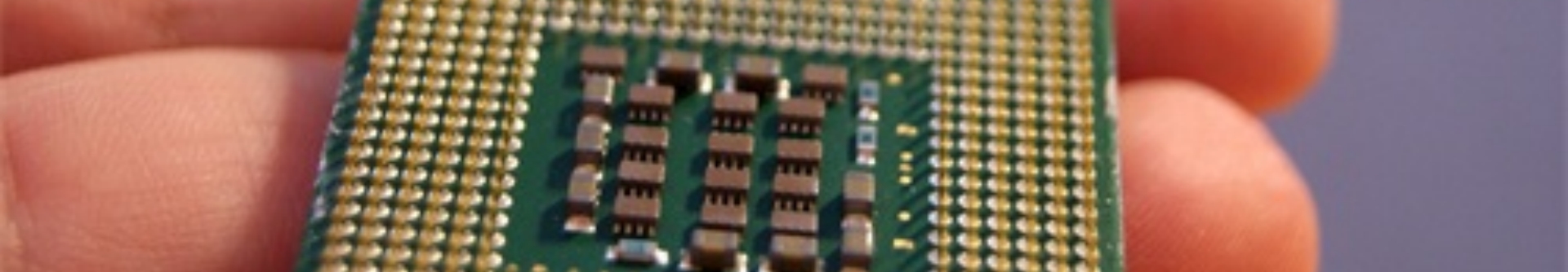
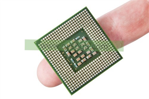
VT 901 Materials Manufacturer
VT 901 Materials Manufacturer,VT 901 料 (プリント基板) represent a cutting-edge class of substrate materials meticulously engineered to elevate PCB performance. Renowned for their exceptional thermal resilience, high dielectric strength, and precise signal transmission properties, VT 901 Materials redefine the standards of reliability and efficiency in electronic circuitry. Tailored for demanding applications spanning aerospace, 電気通信, and automotive industries, these materials epitomize innovation, ensuring robust connectivity, reduced signal loss, and heightened durability. With VT 901 料, PCB designs achieve unprecedented levels of precision and functionality, empowering technological advancements across diverse sectors.
What is a VT 901 料 (プリント基板)?
A VT 901 料 (プリント基板) likely refers to a type of printed circuit board (プリント基板) used in electronic devices. PCBs are crucial components that provide mechanical support and electrical connections between electronic components like resistors, コンデンサー, and integrated circuits. The “VT 901 料” designation could denote specific materials or manufacturing standards used in producing the PCB, which could include the type of substrate material, copper thickness, ソルダーマスク, and other specifications.
PCBs are typically made from materials like fiberglass epoxy resin, with copper traces etched onto the surface to create conductive pathways. These pathways allow electrical signals to flow between components. The specific materials used can impact the performance, 耐久性, and cost of the PCB.
Expanding on this topic, it’s essential to consider factors like the PCB’s layer count, インピーダンス制御, 表面仕上げ, and solderability, as these aspects can affect the functionality and reliability of electronic devices. さらに, advancements in PCB technology, such as flexible and rigid-flex PCBs, have expanded the possibilities for designing smaller, lighter, and more versatile electronic devices.
まとめ, a VT 901 料 (プリント基板) likely denotes a specific type of PCB with designated materials or manufacturing standards, crucial for the performance and reliability of electronic devices. Understanding these specifications is essential for engineers and manufacturers to produce high-quality electronic products.
VT 901 Materials Manufacturer
What are the VT 901 料 (プリント基板) デザインガイドライン?
の設計ガイドライン VT 901 料 (プリント基板) would typically include specifications and recommendations for designing printed circuit boards using these specific materials. While exact guidelines can vary based on the manufacturer or industry standards, some common aspects may include:
- 基板材料: Guidelines may specify the preferred substrate material, such as FR-4 epoxy fiberglass, which is widely used in PCB manufacturing due to its excellent electrical insulation properties and mechanical strength.
- Copper Thickness: Recommendations for copper thickness on the PCB layers, including both outer layers and inner layers, to ensure proper conductivity and signal integrity.
- Trace Width and Spacing: Guidelines for the minimum trace width and spacing between traces to prevent signal interference, クロストーク, and manufacturing issues like etching errors.
- Annular Ring Size: Specifications for the size of annular rings around plated through-holes to ensure proper soldering and electrical connections.
- ソルダーマスク: Recommendations for solder mask application, including the type of solder mask material and its thickness, to protect copper traces and pads while allowing for precise soldering during assembly.
- Silkscreen: Guidelines for silkscreen printing, including text size, font, and placement of component designators, logos, and other markings on the PCB surface.
- Drill Sizes and Tolerances: Specifications for drill sizes and tolerances for plated and non-plated holes, ensuring compatibility with standard component packages and assembly processes.
- 表面仕上げ: Recommendations for surface finish options, such as HASL (熱風はんだレベリング), エニグ (無電解ニッケル浸漬金), or OSP (有機はんだ付け性防腐剤), considering factors like solderability, corrosion resistance, and cost.
- Thermal Considerations: Guidelines for thermal management, including the placement of heat-generating components, サーマルビア, and copper pour areas to dissipate heat effectively and prevent overheating.
- 電気的性能: Specifications for impedance control, シグナルインテグリティ, and EMI (電磁干渉) considerations to ensure the PCB meets performance requirements for high-speed digital or analog circuits.
These guidelines help ensure that PCB designs using VT 901 materials meet quality, 確実, and performance standards, ultimately contributing to the successful manufacture and operation of electronic devices.
What is the VT 901 料 (プリント基板) 製作プロセス?
の製造プロセス VT 901 料 (プリント基板) involves several steps to transform raw materials into finished printed circuit boards ready for electronic assembly. While specific processes can vary based on factors like the complexity of the design and manufacturing equipment used, the following is a general overview of the PCB fabrication process:
- 設計: The process begins with PCB design using specialized software. Designers create the layout of circuit traces, component placements, and other features according to the desired functionality and specifications, including those specific to VT 901 料.
- 基質調製:選択した基板材料, typically FR-4 epoxy fiberglass, is prepared by cutting it to the required size. Surface preparation may involve cleaning and treating the substrate to enhance adhesion during subsequent manufacturing steps.
- Copper Cladding: Copper foil is laminated onto the substrate using heat and pressure to create a conductive layer. This step forms the basis for the circuit traces and conductive pathways on the PCB.
- Lithography:A layer of photosensitive material, called photoresist, is applied to the copper-clad substrate. The PCB design is then transferred onto the photoresist using photomasks and UV light exposure. This process defines the circuit pattern on the copper surface.
- エッチング: The exposed copper areas not protected by the photoresist are chemically etched away, leaving behind the desired circuit traces and features. The remaining photoresist is then stripped off, revealing the copper traces.
- Drilling: Precision holes are drilled into the PCB at locations specified by the design for component mounting and interconnection. These holes are typically plated with copper to provide electrical conductivity between layers if the PCB is multilayered.
- 鍍金: Additional copper plating may be applied to the PCB surface to increase trace thickness or ensure uniformity. Plating can also be used to add other metals like tin or gold for surface finish and solderability.
- ソルダーマスクアプリケーション: A layer of solder mask is applied over the copper traces, leaving only the areas for soldering component leads exposed. Solder mask protects the copper from oxidation and facilitates soldering during assembly.
- Silkscreen Printing: Component designators, logos, and other markings are printed onto the PCB surface using a silkscreen process. This step provides visual guidance for component placement and identification.
- 表面仕上げ: The PCB surface may undergo surface finishing processes like hot air solder leveling (ハスレ), 無電解ニッケル浸漬金 (エニグ), または有機はんだ付け性防腐剤 (OSPの) to improve solderability and protect against corrosion.
- テストと検査: Finished PCBs undergo electrical testing and visual inspection to ensure they meet quality standards and conform to the design specifications.
- Routing and Profiling:Individual PCBs are separated from the manufacturing panel using routing or depanelization methods, and edges are profiled to the final dimensions.
By following these fabrication steps with attention to detail and quality control, manufacturers can produce high-quality VT 901 料 (プリント基板) that meet the required specifications for various electronic applications.
How do you manufacture a VT 901 料 (プリント基板)?
Manufacturing a VT 901 料 (プリント基板) involves several steps, from designing the circuit layout to final quality control checks. Here’s a detailed overview of the manufacturing process:
- Designing the PCB: Engineers create the PCB layout using specialized software, specifying the placement of components, routing of traces, and other design parameters according to the project requirements and VT 901 材料仕様.
- 材料の選択: Choose the appropriate substrate material, typically FR-4 epoxy fiberglass, and copper foil for the PCB construction. Ensure that these materials meet the standards and specifications for VT 901 料.
- Preparation of Substrate: Cut the substrate material to the required size, clean it thoroughly, and treat it to enhance adhesion and surface quality.
- Copper Cladding: Laminate the copper foil onto one or both sides of the substrate using heat and pressure. This step creates a conductive layer that will form the basis for the circuit traces.
- Lithography: Apply a layer of photosensitive material (フォトレジスト) onto the copper-clad substrate. Use photomasks to expose the photoresist to UV light, transferring the PCB design onto it.
- エッチング: Immerse the substrate in an etchant solution, which removes the exposed copper, 目的の回路トレースを残す. Rinse and clean the PCB thoroughly after etching.
- Drilling: Use precision drills to create holes at designated locations on the PCB for component mounting and interconnection. These holes may be plated with copper to provide electrical conductivity between layers in multilayer PCBs.
- 鍍金: 必要 に応じて, apply additional copper plating to the PCB surface to increase trace thickness or ensure uniformity. Other plating processes, such as tin or gold plating, may also be used for surface finish and solderability.
- ソルダーマスクアプリケーション: Apply a layer of solder mask over the PCB surface, leaving openings for soldering component leads. Solder mask protects the copper traces from oxidation and facilitates soldering during assembly.
- Silkscreen Printing: Print component designators, logos, and other markings onto the PCB surface using a silkscreen process. This step provides visual guidance for component placement and identification.
- 表面仕上げ: Apply surface finish treatments such as hot air solder leveling (ハスレ), 無電解ニッケル浸漬金 (エニグ), または有機はんだ付け性防腐剤 (OSPの) to improve solderability and protect against corrosion.
- テストと検査: Conduct electrical testing and visual inspection to ensure that the PCBs meet quality standards and conform to the design specifications. This may include tests for continuity, インピーダンス, and insulation resistance.
- Routing and Profiling: Cut the individual PCBs from the manufacturing panel using routing or depanelization methods. Profile the edges of the PCBs to the final dimensions.
- 梱包と配送: Package the finished PCBs according to customer requirements and prepare them for shipping or further assembly.
By following these steps with precision and attention to detail, manufacturers can produce high-quality VT 901 料 (プリント基板) that meet the necessary standards and specifications for various electronic applications.
How much should a VT 901 料 (プリント基板) 費用?
The cost of a VT 901 料 (プリント基板) can vary widely depending on several factors, including the size, 複雑さ, 量, and specific requirements of the PCB, as well as market conditions and supplier pricing. 一般的に, VT 901 materials may add to the overall cost due to their specific properties or performance characteristics.
Here are some factors that can influence the cost of a VT 901 料 (プリント基板):
- サイズと複雑さ:Larger PCBs with intricate designs and densely populated circuitry typically cost more to manufacture due to increased material and production time.
- レイヤー数: Multilayer PCBs, which have more than two layers of conductive material separated by insulating layers, are more complex to manufacture and generally cost more than single or double-layer PCBs.
- Material Specifications: The choice of VT 901 materials may impact the cost of the PCB. These materials might have specific properties or performance characteristics that make them more expensive than standard materials.
- 製造プロセス: Certain manufacturing processes, such as impedance control, blind and buried vias, and high-precision drilling, can increase production costs.
- Quality Standards: PCBs manufactured to higher quality standards, such as IPC Class 3, may incur additional costs due to stricter quality control measures and testing requirements.
- 量: Economies of scale apply in PCB manufacturing, meaning that larger quantities typically result in lower unit costs. しかし, setup costs may offset these savings for small production runs.
- リード タイム: Shorter lead times often incur rush fees or expedited shipping costs, which can increase the overall price of the PCB
- Supplier Selection: Different PCB manufacturers may offer varying pricing based on their capabilities, 備品, 場所, and business model.
It’s essential to obtain quotes from multiple PCB manufacturers and consider all relevant factors when estimating the cost of VT 901 料 (プリント基板) for a specific project. かつ, engaging in a dialogue with suppliers to discuss requirements and potential cost-saving strategies can help optimize the overall procurement process.
What is VT 901 料 (プリント基板) base material?
VT 901 料 (プリント基板) likely refers to a specific type of base material used in the fabrication of printed circuit boards (プリント基板). While there isn’t a standard definition for VT 901 料, it’s possible that it denotes a particular set of material specifications or standards designated by a manufacturer or industry.
In the context of PCB fabrication, the base material serves as the foundation upon which the conductive traces and components are built. The choice of base material significantly impacts the performance, 確実, and cost of the PCB. Here are some common base materials used in PCB manufacturing:
- FR-4 Epoxy Fiberglass: This is the most widely used base material in PCB fabrication. FR-4 (Fire Retardant 4) is a type of flame-retardant glass-reinforced epoxy laminate. It offers excellent electrical insulation properties, 機械的強度, と寸法安定性. FR-4 is suitable for a wide range of applications and is available in various thicknesses and copper weights.
- FR-1 and FR-2 Paper Phenolic: These materials are less common than FR-4 but are still used in certain applications. FR-1 and FR-2 are paper-based substrates impregnated with phenolic resin and are typically less expensive than FR-4. しかし, they have lower mechanical strength and moisture resistance compared to FR-4.
- Metal Core PCBs (MCPCB): In MCPCBs, the base material is typically aluminum or copper instead of fiberglass. These materials offer superior thermal conductivity, 効率的な熱放散を必要とするアプリケーションに適しています, LED照明やパワーエレクトロニクスなど.
- High-Frequency Materials: For RF (無線周波数) and microwave applications, specialized base materials with low dielectric constant and low loss tangent are used to minimize signal loss and maintain signal integrity at high frequencies.
- Flexible and Rigid-Flex Materials: Flex PCBs and rigid-flex PCBs use flexible base materials such as polyimide (例えば。, カプトン) or polyester (例えば。, ペット) instead of rigid substrates. These materials enable PCBs to bend or flex, making them suitable for applications with space constraints or requiring repeated flexing.
- Specialty Materials: Certain applications may require specialty base materials with specific properties, such as high-temperature resistance, 耐薬品性, or reduced flammability. These materials may include polytetrafluoroethylene (PTFE製), ceramic-filled laminates, or composite materials.
While the term “VT 901 料” doesn’t specify a particular base material, it likely refers to a set of material specifications, スタンダーズ, or proprietary formulations designated by a manufacturer or industry. These specifications may include parameters such as dielectric constant, dissipation factor, 熱伝導率, と寸法安定性, tailored to meet the requirements of specific applications or performance standards.
When selecting a base material for PCB fabrication, designers and manufacturers must consider factors such as electrical performance, 機械的強度, サーマルマネジメント, 費用, and environmental considerations to ensure the PCB meets the desired specifications and performance requirements. かつ, adherence to industry standards such as IPC (一般社団法人 エレクトロニクス産業をつなぐ協会) specifications ensures consistency and quality in PCB manufacturing.
Which company makes VT 901 料 (プリント基板)?
現在は, there is no specific company that is explicitly mentioned as manufacturing VT 901 料 (プリント基板). しかし, VT 901 Materials may refer to a particular type of PCB substrate rather than a specific company. This means it could be a set of material standards or specifications used by multiple PCB manufacturers.
As a PCB manufacturer, our company can produce VT 901 料 (プリント基板) according to customer requirements. We have advanced production equipment and a skilled technical team capable of meeting various PCB design and manufacturing needs. Our manufacturing process includes every step from PCB design to final quality control to ensure the production of high-quality PCBs that meet customer specifications.
Our manufacturing capabilities include, ただし、これらに限定されません:
- Various Material Selection: We can use different types of base materials according to customer requirements, including FR-4 epoxy fiberglass, metal substrates (アルミニウムや銅など), and high-frequency materials to meet different application needs.
- 高精度な製造: With advanced processing equipment and precise process control capabilities, we can produce PCBs with complex wiring and high-density component layouts.
- 厳格な品質管理: We adhere to rigorous quality management systems, including strict control of raw materials, multiple quality inspections during the production process, and comprehensive testing and inspection before shipment to ensure the production of high-quality products.
- カスタマイズサービス: We offer customized services to meet specific customer requirements, including special process requirements and material needs, to meet the unique needs of different customers.
- Timely Delivery:We have flexible production resource allocation to ensure on-time delivery of customer orders. かつ, we offer expedited services to meet the urgent needs of customers.
まとめ, as a professional PCB manufacturer, our company has the technical capabilities and manufacturing experience to produce VT 901 料 (プリント基板). We are committed to providing customers with high-quality and reliable PCB products and offer customized production services to meet specific customer requirements.
は何ですか 7 優れたカスタマーサービスの品質?
Good customer service is characterized by several key qualities that contribute to a positive experience for customers. Here are seven qualities of good customer service:
- 応答: Good customer service involves being prompt and proactive in addressing customer inquiries, 懸念, とリクエスト. Responding promptly to customer needs demonstrates attentiveness and a commitment to providing timely assistance.
- 共感: Empathy involves understanding and acknowledging the customer’s perspective, feelings, and needs. Customer service representatives should demonstrate empathy by actively listening to customers, expressing understanding of their concerns, and showing genuine care and concern for their well-being.
- 明瞭さとコミュニケーション: Effective communication is essential for good customer service. カスタマーサービス担当者は、明確かつ簡潔にコミュニケーションをとる必要があります, using language that is easy for customers to understand. They should provide accurate information, 指示, and updates to help customers resolve issues or make informed decisions.
- プロ 意識: Professionalism entails maintaining a courteous, 恭しい, and positive demeanor when interacting with customers. カスタマーサービス担当者は、常にプロフェッショナルに振る舞う必要があります, regardless of the situation or the customer’s behavior. This includes being patient, polite, and maintaining a professional tone of voice and demeanor.
- 知識能力: Good customer service requires having a thorough understanding of the products or services offered, as well as company policies, procedures, and protocols. Customer service representatives should be knowledgeable and well-trained to provide accurate information, answer questions, and assist customers effectively.
- 問題解決スキル: Effective problem-solving skills are crucial for resolving customer issues and concerns. Customer service representatives should be proactive in identifying and addressing customer problems, finding solutions, and taking appropriate action to resolve issues to the customer’s satisfaction.
- Consistency: Consistency is key to providing a positive and reliable customer service experience. Customer service standards, policies, and procedures should be consistently applied across all interactions and touchpoints. Consistency helps build trust and confidence in the company’s commitment to delivering high-quality customer service.
これらの資質を具現化することで、, businesses can cultivate strong relationships with their customers, ロイヤリティを育む, and differentiate themselves in the competitive marketplace.
よくあるご質問(FAQ)
What are VT 901 料 (プリント基板)?
VT 901 Materials likely refer to a specific set of materials or material standards used in the fabrication of printed circuit boards (プリント基板). These materials may have particular properties or characteristics tailored to meet certain performance requirements or specifications.
What are the properties of VT 901 料 (プリント基板)?
The properties of VT 901 Materials can vary depending on the specific materials or standards they encompass. 一般的に, VT 901 Materials may include characteristics such as high thermal resistance, 優れた電気絶縁性, 低誘電率, or specific mechanical properties tailored for demanding applications.
What applications are VT 901 料 (プリント基板) suitable for?
VT 901 料 (プリント基板) may be suitable for various applications, including high-speed digital circuits, RF/microwave systems, パワーエレクトロニクス, 航空宇宙および防衛, 自動車用電子機器, and other industries requiring high-performance PCBs with specific material properties.
Are VT 901 料 (プリント基板) more expensive than standard materials?
The cost of VT 901 料 (プリント基板) can vary depending on the specific materials, 製造プロセス, and performance requirements. 場合によっては, VT 901 Materials may be more expensive than standard materials due to their specialized properties or performance characteristics.
Can any PCB manufacturer produce VT 901 料 (プリント基板)?
Not necessarily. VT 901 料 (プリント基板) may require specific expertise, 備品, and manufacturing processes to meet the required specifications. It’s essential to work with a PCB manufacturer with experience and capabilities in handling specialized materials and meeting performance standards.
What standards or specifications define VT 901 料 (プリント基板)?
The specific standards or specifications defining VT 901 Materials may vary depending on the industry or application requirements. It’s essential to consult with the manufacturer or refer to industry standards such as IPC (一般社団法人 エレクトロニクス産業をつなぐ協会) specifications for detailed information.
Can VT 901 料 (プリント基板) be customized for specific applications?
はい, VT 901 料 (プリント基板) can often be customized to meet the specific performance requirements or application needs of customers. This may include adjustments to material properties, 厚さ, レイヤー構成, or other parameters to optimize PCB performance for a particular application.
What are the advantages of using VT 901 料 (プリント基板)?
The advantages of VT 901 料 (プリント基板) may include improved signal integrity, サーマルマネジメント, 確実, and overall performance compared to standard materials. These materials are often chosen for applications where exceptional performance and reliability are critical.