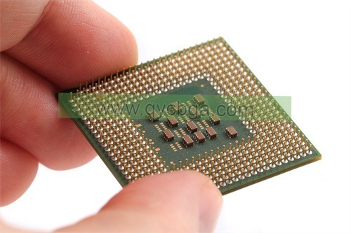
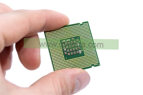
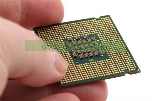
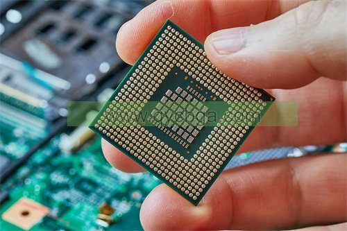
What is 3D IC Package Substrate?
3D ICパッケージ基板メーカー,3Dアイシー (集積回路) package substrate is an innovative technology enabling stacked semiconductor dies in a single package, enhancing performance and density. This substrate facilitates vertical integration of chips, reducing interconnect length and improving signal speed. By stacking chips, 3D IC substrates optimize space utilization and enhance thermal management. Commonly made from materials like silicon interposers or advanced laminates, they offer reliable electrical performance and mechanical stability. Widely used in high-performance computing, 人工知能, データセンター, 3D IC package substrates drive advancements in semiconductor packaging, enabling smaller form factors and higher processing power in electronic devices.
A 3D IC package substrate is a key component in three-dimensional integrated circuit (3Dアイシー) テクノロジー. In traditional integrated circuits (ICの), electronic components are arranged side by side on a single layer. しかし, in 3D IC technology, multiple layers of ICs are stacked vertically to increase functionality and performance while reducing the overall footprint.
The 3D IC package substrate serves as a platform for connecting and interconnecting the stacked IC layers. It provides electrical connections between the different layers of ICs, as well as between the ICs and external components such as the printed circuit board (プリント基板) またはその他のシステムコンポーネント.
These substrates are designed to handle the increased heat dissipation and electrical demands associated with 3D IC integration. They often incorporate advanced materials and manufacturing techniques to achieve the necessary performance, 確実, and thermal management requirements.
全, the 3D IC package substrate plays a critical role in enabling the integration of multiple IC layers in a compact and efficient manner, thereby facilitating the development of high-performance electronic systems.

3D ICパッケージ基板メーカー
3D IC Package Substrate design Reference Guide.
デザイン 3D IC package substrate 最適なパフォーマンスを確保するためには、さまざまな要素を慎重に検討する必要があります, 確実, と製造可能性. Here’s a reference guide covering key aspects of 3D IC package substrate design:
- 材料の選択: Choose substrate materials with suitable electrical, 熱の, および機械的特性. 一般的な材料には有機基板が含まれます (例えば。, FR-4), セラミック基板, and advanced materials like silicon interposers or glass interposers.
- Interconnection Technology: Select appropriate interconnection technologies such as through-silicon vias (TSVの), microbumps, はんだボール, or copper pillars. Each technology has its advantages and limitations in terms of pitch, density, と信頼性.
- Routing Architecture: Design an efficient routing architecture to facilitate high-speed signal transmission and minimize signal integrity issues such as crosstalk and impedance mismatch. Consider the placement and routing of TSVs, microbumps, and signal traces to optimize electrical performance.
- 電力供給ネットワーク (PDNの): Design a robust power delivery network to ensure adequate power distribution and thermal management. Incorporate power planes, デカップリングコンデンサ, and thermal vias to mitigate power noise and heat dissipation issues.
- シグナルインテグリティ (SIの) and Electromagnetic Interference (EMIの): Perform SI and EMI analysis to identify and mitigate potential signal integrity and electromagnetic compatibility issues. Utilize signal and power integrity simulation tools to optimize the substrate layout and stackup.
- サーマルマネジメント: Implement effective thermal management techniques to dissipate heat generated by the stacked IC layers. サーマルビアを内蔵, ヒートスプレッダー, and thermal interface materials to enhance heat dissipation and thermal conductivity.
- Package Size and Form Factor: Determine the appropriate package size and form factor based on system requirements, including space constraints, electrical performance goals, and integration complexity.
- 信頼性に関する考慮事項: 機械的ストレスなどの信頼性の懸念に対処する, サーマルサイクル, and solder joint fatigue. Perform reliability simulations and testing to validate the substrate design under various operating conditions.
- Manufacturability and Cost: Optimize the substrate design for manufacturability and cost-effectiveness. Consider factors such as substrate fabrication processes, yield optimization, and assembly techniques to streamline production and minimize manufacturing costs.
- Compliance and Standards: Ensure compliance with industry standards and regulations governing substrate materials, interconnection technologies, and electrical performance specifications.
By carefully addressing these design considerations, engineers can develop 3D IC package substrates that meet the performance, 確実, and cost requirements of advanced electronic systems. Collaboration with substrate suppliers, semiconductor manufacturers, and system integrators is essential to leverage expertise and resources throughout the design process.
What are the materials used in 3D IC Package Substrate?
Several materials are used in the construction of 3D IC package substrates, each offering unique properties suited to specific requirements. Here are some common materials used:
- 有機基質: Organic substrates such as FR-4 (難燃 4) are widely used in traditional PCBs and can also be employed in 3D IC package substrates. FR-4 is cost-effective, lightweight, and offers good electrical insulation properties. しかし, it may have limitations in terms of thermal conductivity and reliability at higher temperatures.
- セラミック基板: セラミック基板, typically made of alumina (Al2O3) または窒化アルミニウム (AlNの), は、その優れた熱伝導率で知られています, 機械的強度, と信頼性. Ceramic substrates are well-suited for applications requiring high power dissipation and thermal management.
- シリコンインターポーザー: Silicon interposers are silicon wafers with through-silicon vias (TSVの) that provide vertical interconnections between stacked IC layers. Silicon interposers offer high electrical performance, 低寄生容量, and compatibility with standard semiconductor processes. They are often used in high-performance applications such as advanced microprocessors and memory devices.
- Glass Interposers: Glass interposers are fabricated using glass substrates with TSVs for vertical interconnections. Glass interposers offer advantages such as low cost, 高い電気絶縁性, and compatibility with large-scale manufacturing processes. They are suitable for applications requiring high-density interconnects and signal integrity.
- Polymer Interposers: Polymer interposers are made of polymer materials such as polyimide or liquid crystal polymer (LCPの). Polymer interposers offer flexibility, low cost, and ease of processing compared to ceramic and silicon substrates. They are suitable for applications requiring moderate electrical performance and interconnect density.
- 金属基板: Metal substrates such as copper or aluminum can be used as carriers or heat spreaders in 3D IC packaging. Metal substrates offer high thermal conductivity and mechanical strength, making them suitable for thermal management in high-power applications.
- フレキシブル基板: Flexible substrates made of polyimide or other flexible materials are used in applications requiring bendable or stretchable electronics. Flexible substrates offer versatility and conformability to irregular shapes, making them suitable for wearable devices and flexible displays.
The choice of substrate material depends on various factors including electrical performance requirements, 熱管理のニーズ, コストに関する考慮事項, and specific application demands. Designers must carefully evaluate these factors to select the most appropriate substrate material for their 3D IC packaging design.
How is 3D IC Package Substrate manufactured?
Manufacturing 3D IC package substrates involves several intricate processes aimed at creating a robust substrate capable of accommodating multiple stacked IC layers and facilitating efficient electrical connections. Here’s an overview of the typical manufacturing steps:
- 基板製造: このプロセスは、基板材料の製造から始まります. 選択した材料によって異なります (例えば。, organic, セラミック, silicon, グラス), this may involve techniques such as lamination, deposition, or casting to create the substrate’s base layer.
- ビアフォーメーション: For substrates requiring vertical interconnections (例えば。, シリコンインターポーザー, glass interposers), through-silicon vias (TSVの) or through-glass vias (TGVs) are formed. This process involves etching or drilling holes through the substrate material and filling them with conductive material such as copper or tungsten to establish electrical pathways between stacked IC layers.
- 表面処理: The substrate surface is prepared for subsequent processes such as metallization and bonding. This may involve cleaning, surface activation, and chemical treatment to ensure optimal adhesion and compatibility with subsequent layers.
- メタライゼーション: Metal layers are deposited onto the substrate surface to create conductive traces, パッド, および相互接続. Techniques such as physical vapor deposition (PVDディスプレイ) または化学蒸着 (CVD検出器) are used to deposit metals such as copper, aluminum, or gold onto the substrate surface.
- Dielectric Deposition: Dielectric layers are deposited onto the substrate surface to insulate and protect the underlying metallization layers. Dielectric materials such as polyimide, 二酸化ケイ素, or benzocyclobutene (BCBの) are commonly used for this purpose. These layers may also incorporate vias for vertical interconnections.
- Interconnect Formation: The process of forming interconnects between the substrate and the stacked IC layers begins. This may involve techniques such as flip-chip bonding, soldering, or thermo-compression bonding to establish electrical connections between the substrate and the ICs.
- Assembly and Stacking: Once the substrate is prepared, IC chips are assembled onto the substrate surface using precision placement techniques. Multiple IC layers may be stacked on top of each other, with interconnections established through TSVs or other vertical interconnect technologies.
- Encapsulation and Packaging: The assembled substrate and stacked IC layers are encapsulated and packaged to protect them from environmental factors such as moisture, 塵, と機械的ストレス. This may involve techniques such as molding, underfilling, or encapsulation with epoxy resins or polymers.
- テストと品質保証: The completed 3D IC package substrates undergo rigorous testing and quality assurance procedures to ensure they meet electrical performance, 確実, and durability requirements. これには、電気テストが含まれる場合があります, サーマルサイクル, and mechanical stress testing.
- Final Inspection and Packaging: Once testing is completed, the finished 3D IC package substrates are inspected for defects and packaged for shipment to customers or further assembly into electronic systems.
製造プロセス全体を通じて, stringent process controls, quality assurance measures, and advanced metrology techniques are employed to ensure the reliability, パフォーマンス, and consistency of the 3D IC package substrates. Collaboration among substrate manufacturers, semiconductor foundries, and assembly partners is often required to optimize the manufacturing process and meet the demanding requirements of advanced electronic systems.
The Application area of 3D IC Package Substrate
The application areas of 3D IC package substrates span a wide range of industries and technologies, driven by the need for enhanced performance, 小型化, and integration capabilities. Some key application areas include:
- ハイパフォーマンスコンピューティング (HPCの): In HPC systems, such as supercomputers and data centers, 3D IC package substrates enable the integration of multiple processors, memory modules, and accelerators in a compact form factor. This results in increased computational power, レイテンシーの低減, and improved energy efficiency.
- Telecommunications and Networking: 3D IC package substrates are used in telecommunications and networking equipment to enhance data processing and routing capabilities. By stacking multiple ICs vertically, these substrates enable the development of high-speed routers, スイッチ, and base stations with improved throughput and scalability.
- 家電: In consumer electronics devices such as smartphones, 錠剤, およびウェアラブル, 3D IC package substrates enable the integration of multiple functionalities in a compact and lightweight form factor. This allows for the development of feature-rich devices with improved performance, battery life, and form factor.
- カーエレクトロニクス: 自動車業界, 3D IC package substrates are utilized in advanced driver assistance systems (ADASの), インフォテインメントシステム, およびエンジン制御ユニット (ECU(エキュエート). These substrates enable the integration of sensors, processors, およびメモリモジュール, leading to enhanced safety, efficiency, and connectivity in vehicles.
- 医療機器: 医療機器および機器に, 3D IC package substrates enable the development of compact and portable solutions for diagnostic imaging, patient monitoring, and therapeutic applications. By integrating multiple functions and sensors, these substrates facilitate the development of advanced medical technologies with improved accuracy and reliability.
- 航空宇宙・防衛: 航空宇宙および防衛用途, 3D IC package substrates are used in radar systems, アビオニクス, and communication systems. These substrates enable the integration of complex electronics in space-constrained environments, leading to improved performance, 確実, and ruggedness.
- インダストリアル・オートメーション: In industrial automation and control systems, 3D IC package substrates enable the development of compact and energy-efficient solutions for process control, ロボティックス, and machine vision. By integrating multiple sensors, アクチュエータ, and processing units, these substrates enhance productivity, 柔軟性, and efficiency in manufacturing environments.
- Emerging Technologies: 3D IC package substrates are also being explored for emerging technologies such as Internet of Things (IoTの), 人工知能 (AI), and augmented reality (AR)/virtual reality (VR). These substrates enable the integration of diverse functionalities and sensors, paving the way for innovative applications and services in various industries.
全, the application areas of 3D IC package substrates continue to expand as technology advancements drive the demand for higher performance, 統合, and miniaturization in electronic systems across diverse industries.
What are the advantages of 3D IC Package Substrate?
3D IC package substrates offer several advantages over traditional 2D packaging solutions, making them increasingly popular for advanced electronic systems. 主な利点には、次のようなものがあります:
- Increased Performance: By vertically stacking multiple IC layers, 3D IC package substrates reduce interconnect lengths and enable shorter signal pathways. This leads to reduced signal propagation delays, 低消費電力, and higher operating speeds, resulting in improved overall system performance.
- Enhanced Integration: 3D IC package substrates facilitate the integration of multiple functionalities, プロセッサなど, 記憶, センサー, and RF components, within a compact form factor. This enables the development of highly integrated systems-on-chip (SoCs) およびシステムインパッケージ (一口) solutions with reduced footprint and improved functionality.
- Higher Bandwidth and Connectivity: Vertical integration in 3D IC package substrates allows for denser interconnects and increased bandwidth between stacked IC layers. This enables faster data transfer rates, improved data throughput, and enhanced connectivity, making them ideal for high-speed communication and data processing applications.
- Improved Power Efficiency: With shorter interconnect lengths and reduced parasitic capacitance, 3D IC package substrates offer improved power efficiency compared to traditional 2D packaging solutions. This leads to lower power consumption, reduced heat generation, and extended battery life in portable and battery-powered devices.
- サーマルマネジメント: 3D IC package substrates facilitate efficient thermal management by providing a shorter thermal path between the stacked IC layers and external heat sinks. This helps dissipate heat more effectively, mitigating thermal hotspots and improving overall system reliability and longevity.
- Miniaturization and Form Factor Flexibility: By stacking IC layers vertically, 3D IC package substrates enable miniaturization of electronic systems and components, allowing for smaller and more compact designs. This flexibility in form factor enables the development of innovative products for various applications, including wearables, IoTデバイス, および自動車用電子機器.
- Heterogeneous Integration: 3D IC package substrates support heterogeneous integration, allowing for the integration of different types of ICs, 技術, と1つのパッケージ内の材料. This enables the co-packaging of diverse functionalities, such as digital, analog, RFの, and MEMS components, to meet the specific requirements of complex electronic systems.
- Cost Savings and Yield Improvement: While initial manufacturing costs may be higher for 3D IC package substrates due to the complexity of fabrication processes, これにより、製品ライフサイクル全体でコストを削減できます. This is achieved through reduced component count, 組み立てプロセスの簡素化, and improved yield due to smaller form factors and higher integration levels.
全, the advantages of 3D IC package substrates, including improved performance, 統合, 電力効率, and form factor flexibility, make them an attractive choice for a wide range of advanced electronic applications.
How Much Does 3D IC Package Substrate Cost?
The cost of 3D IC package substrates can vary significantly depending on various factors such as the chosen substrate material, manufacturing complexity, design requirements, and volume production considerations. ここでは、コストに影響を与える主な要因をいくつか紹介します:
- 基板材料: Different substrate materials have different costs associated with their production. 例えば, organic substrates (例えば。, FR-4) are generally more cost-effective compared to ceramic, silicon, or glass substrates, which may require more sophisticated manufacturing processes and materials.
- Manufacturing Complexity: The complexity of the manufacturing process can impact the cost of 3D IC package substrates. Processes such as via formation, メタライゼーション, インターコネクトフォーメーション, and stacking may require specialized equipment, 料, and expertise, which can contribute to higher manufacturing costs.
- Design Requirements: The complexity and sophistication of the substrate design, including features such as via density, トレースルーティング, interconnect pitch, and thermal management solutions, can influence the cost of fabrication. More complex designs may require additional manufacturing steps and materials, コストの上昇につながる.
- 量産: The economies of scale associated with volume production can significantly impact the cost of 3D IC package substrates. Higher production volumes typically lead to lower per-unit costs due to efficiencies in manufacturing processes, materials procurement, および諸経費.
- Technology Node and Yield Rates: The adoption of advanced semiconductor processes and technologies, such as smaller feature sizes and higher interconnect densities, may increase manufacturing costs initially. しかし, as these technologies mature and yield rates improve, the cost per unit may decrease over time.
- Supplier Relationships and Supply Chain Factors: The relationships with substrate suppliers, semiconductor foundries, 組立パートナー, and other supply chain stakeholders can influence the overall cost of 3D IC package substrates. Collaborative partnerships and strategic sourcing initiatives may help optimize costs and improve competitiveness.
- Market Dynamics and Competition: 市場の需要, industry trends, and competitive dynamics can also impact the pricing of 3D IC package substrates. Pricing may fluctuate based on supply and demand dynamics, competitive pressures, and technological advancements within the industry.
全, while it’s challenging to provide a specific cost figure for 3D IC package substrates due to the numerous variables involved, it’s essential for stakeholders to carefully evaluate cost considerations alongside performance, 確実, and other factors when selecting substrate materials and manufacturing processes for their applications.
FAQs about 3D IC Package Substrate
What is a 3D IC package substrate?
A 3D IC package substrate is a component used in three-dimensional integrated circuit (3Dアイシー) テクノロジー. It serves as a platform for connecting and interconnecting multiple stacked IC layers, facilitating high-performance electronic systems in a compact form factor.
How does a 3D IC package substrate differ from traditional IC packaging?
Unlike traditional IC packaging, which involves arranging electronic components side by side on a single layer, 3D IC package substrates enable the vertical stacking of multiple IC layers. This allows for increased functionality, パフォーマンス, and integration while reducing the overall footprint.
What are the advantages of using a 3D IC package substrate?
Some advantages of 3D IC package substrates include increased performance, enhanced integration, improved power efficiency, better thermal management, and flexibility in form factor design.
What materials are used in 3D IC package substrates?
Common materials used in 3D IC package substrates include organic substrates (例えば。, FR-4), セラミック基板, シリコンインターポーザー, glass interposers, polymer interposers, and metal substrates.
How are 3D IC package substrates manufactured?
The manufacturing process for 3D IC package substrates involves substrate fabrication, via formation, 表面処理, メタライゼーション, dielectric deposition, インターコネクトフォーメーション, assembly and stacking, encapsulation and packaging, testing and quality assurance, and final inspection and packaging.
What are the applications of 3D IC package substrates?
3D IC package substrates find applications in various industries and technologies, ハイパフォーマンスコンピューティングを含む, 電気通信, 家電, 自動車用電子機器, 医療機器, 航空宇宙および防衛, 産業オートメーション, and emerging technologies such as IoT, AI, and AR/VR.
How much does a 3D IC package substrate cost?
The cost of 3D IC package substrates can vary depending on factors such as substrate material, manufacturing complexity, design requirements, volume production considerations, technology node, yield rates, サプライヤーとの関係, and market dynamics.
What are some key considerations when designing with 3D IC package substrates?
Important design considerations include material selection, interconnection technology, routing architecture, power delivery network (PDNの), シグナルインテグリティ (SIの) および電磁干渉 (EMIの), サーマルマネジメント, package size and form factor, 信頼性に関する考慮事項, 製造可能性, compliance and standards.
 FCBGAパッケージ基板メーカー

