
Flip Chip BGA Substrates Manufacturer
Flip Chip BGA Substrates Manufacturer,Flip Chip BGA Substrates are advanced packaging solutions in the semiconductor industry. They facilitate direct mounting of flip chips onto substrates, enhancing electrical performance and reliability. By connecting the chip’s active side to the substrate through solder bumps, these substrates offer improved signal integrity and thermal management. They find applications in high-performance computing, 電気通信, 自動車用電子機器, その他. Manufactured using materials like FR4, BT resin, or polyimide, Flip Chip BGA Substrates undergo rigorous quality control to ensure optimal functionality. 全, they enable compact, high-density electronic designs, crucial for modern electronic devices.
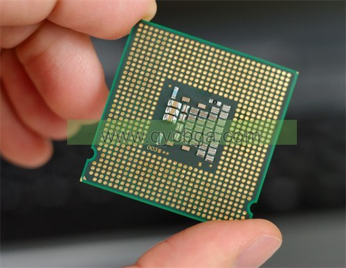
What are Flip Chip BGA Substrates?
フリップチップボールグリッドアレイ (BGAの) substrates are an advanced type of packaging technology used in the semiconductor industry to mount and connect flip chips to printed circuit boards (プリント基板). A flip chip is a type of integrated circuit (集積回路) that is mounted directly onto the substrate or the PCB with its active side facing downward, unlike traditional wire-bonded chips where connections are made on the perimeter of the chip.
The “flip” aspect of the flip chip involves turning the silicon chip upside down so that its electrical connections are facing the substrate, which allows for a more direct path for electrical signals and can reduce signal path lengths significantly. This orientation enhances the performance characteristics of the device, such as increased speed and reduced interference, which are crucial in high-performance computing applications.
The BGA aspect of the substrate refers to the method used to mount the chip onto the PCB. BGA packages use tiny solder balls arranged in a grid pattern on the underside of the substrate. These solder balls are used to electrically connect the chip to the PCB when the whole assembly is heated and the solder reflows, creating a reliable mechanical and electrical connection. The substrate itself is a crucial part of this package, serving as the intermediary that carries the electrical signals from the chip to the solder balls.
These substrates are typically made from materials like FR4, BT resin, or polyimide, depending on the performance requirements, such as thermal stability, 電気絶縁性, と機械的強度. They often contain multiple layers that can include power, グランドプレーン, and signal traces to manage the complex routing required for high-density connections.
全, Flip Chip BGA substrates enable more efficient, compact, and high-performance chip designs, which are essential for modern electronic devices that demand high-speed data processing and minimal power consumption.
Flip Chip BGA Substrates Manufacturer
What are the Flip Chip BGA Substrates Design Guidelines?
Designing Flip Chip Ball Grid Array (BGAの) 基板 involves meticulous planning and adherence to specific guidelines to ensure reliability, パフォーマンス, と製造可能性. The design of these substrates is critical because they need to effectively integrate the flip chip with the rest of the electronic system, particularly for high-performance applications. Here are several key guidelines typically followed in the design of Flip Chip BGA substrates:
- 材料の選択: The choice of substrate material affects the thermal, メカニカル, and electrical properties of the package. Materials such as high-performance FR4, BT resin, or polyimide are common, chosen based on their thermal stability and electrical insulation properties.
- サーマルマネジメント: Effective heat dissipation is crucial in flip chip designs to ensure reliable performance and longevity. Designers must incorporate features such as thermal vias, ヒートスプレッダー, or thermal interface materials to manage the heat generated by the chip.
- Pad Design: The design of the solder pads on the substrate must match the bump pattern on the flip chip. This includes considerations for pad size, pitch, and the type of solder mask used. Pad design affects solder joint reliability, which is critical for the overall robustness of the package.
- シグナルインテグリティ: High-speed signals require careful routing to minimize delay and signal distortion. This involves controlling the impedance of signal traces, managing crosstalk, and ensuring proper signal isolation. Multiple routing layers might be used to achieve optimal signal integrity.
- 配電ネットワーク (PDNの) 設計: Adequate power delivery must be ensured to all parts of the chip. This involves designing a robust power distribution network that can handle the current requirements and minimize voltage drops across the substrate.
- I/O Routing: The layout must ensure that all inputs and outputs are accessible and correctly routed to minimize latency and interference. This might involve complex layer designs and the use of blind and buried vias.
- 機械的安定性:The substrate must be mechanically stable to handle stress during assembly and operation. This involves considering the coefficient of thermal expansion (CTEの) of the substrate material in relation to the chip and the PCB to which it will be attached.
- Assembly and Manufacturing Constraints: The design must also consider manufacturability. This includes ensuring that the design adheres to the capabilities of the assembly equipment, such as alignment accuracy, solder paste printing, and reflow soldering processes.
- Testing and Accessibility: Provisions for testing and debugging, such as test pads or probe points, should be incorporated into the design to facilitate easy inspection and testing during and after manufacturing.
- 信頼性に関する考慮事項: The substrate design should comply with industry standards for reliability, which may involve simulations and testing for conditions such as thermal cycling, drop impact, and moisture absorption.
これらのガイドラインに従う, designers can optimize Flip Chip BGA substrates for functionality, 確実, とパフォーマンス, addressing the demands of modern electronic devices and systems. These guidelines are also often supplemented by specific requirements from semiconductor companies and OEMs, adapting to new technologies and materials.
What is the Flip Chip BGA Substrates Fabrication Process?
The fabrication process of Flip Chip Ball Grid Array (BGAの) 基板 involves several steps to create a reliable and high-performance package for semiconductor devices. While specific processes may vary depending on factors such as the substrate material and the requirements of the application, the general steps typically include:
- 基質調製: The process begins with preparing the substrate material, which is often a laminate composed of multiple layers of materials such as FR4, BT resin, or polyimide. The substrate may be pre-drilled with vias or through-holes depending on the design requirements.
- 表面処理: The substrate surface is cleaned and treated to ensure proper adhesion of subsequent layers and the solder bumps.
- 回路パターニング: Circuit patterns are defined on the substrate using lithography and etching techniques. This involves depositing a thin layer of conductive material (銅など) onto the substrate surface and then selectively removing the material to create the desired traces, パッド, とビア.
- Dielectric Layer Deposition: Insulating dielectric layers are deposited over the circuit patterns to electrically isolate different layers and provide mechanical support.
- ビアフォーメーション: Vias are created to establish electrical connections between different layers of the substrate. This may involve drilling holes through the substrate and then filling them with conductive material or using laser drilling techniques for smaller vias.
- Conductor Deposition:Additional layers of conductive material are deposited onto the substrate surface to create the interconnects and pads necessary for connecting the flip chip to the substrate.
- ソルダーマスクアプリケーション: はんだマスク層が基板表面に塗布されます, leaving openings for the solder bumps and contact pads. The solder mask helps protect the substrate and defines the areas where solder will be applied during assembly.
- 表面仕上げ: Surface finish processes such as electroless nickel immersion gold (エニグ), 有機はんだ付け性防腐剤 (OSPの), or immersion tin are applied to the contact pads to improve solderability and prevent oxidation.
- Bump Placement: Solder bumps are applied to the contact pads on the substrate using processes such as solder paste stencil printing, solder jetting, or electroplating. These bumps serve as the electrical connections between the flip chip and the substrate.
- Flip Chip Attachment: The flip chip is precisely aligned and mounted onto the substrate, with the solder bumps making contact with corresponding pads on the substrate. This process may involve using alignment tools and reflow soldering techniques to ensure proper attachment.
- アンダーフィルカプセル化:An underfill material is applied between the flip chip and the substrate to provide mechanical support and improve reliability by reducing stresses during thermal cycling. The underfill material is typically dispensed and cured under heat.
- Quality Control and Testing: The fabricated substrates undergo rigorous testing to ensure that they meet the required specifications for electrical connectivity, 機械的完全性, と信頼性. This may involve visual inspection, 電気試験, and reliability testing under various environmental conditions.
次の手順に従います, manufacturers can fabricate Flip Chip BGA substrates that meet the demanding requirements of modern semiconductor devices and electronic systems. Continuous advancements in materials and processes contribute to improved performance, 確実, and manufacturability of these substrates.
How do you manufacture Flip Chip BGA Substrates?
Manufacturing Flip Chip Ball Grid Array (BGAの) substrates involves a series of intricate processes aimed at creating robust and high-performance packaging solutions for semiconductor devices. Here’s an overview of the typical steps involved in the manufacturing process:
- 基板材料選定: The process begins with selecting the appropriate substrate material based on factors such as thermal performance, 電気的特性, と機械的強度. Common substrate materials include FR4, BT resin, or polyimide.
- 基板製造: The selected substrate material undergoes fabrication processes such as lamination, 錬成, and layer alignment to create the base substrate with the desired number of layers and dimensions. This involves bonding multiple layers of substrate material together to form a solid structure.
- 表面処理: The substrate surface is cleaned and treated to remove any contaminants and ensure proper adhesion of subsequent layers and components.
- 回路パターニング: Circuit patterns are defined on the substrate using photolithography and etching techniques. A thin layer of conductive material (typically copper) is deposited onto the substrate surface, and then the excess material is selectively removed to create the desired traces, パッド, とビア.
- Dielectric Layer Deposition: Insulating dielectric layers are deposited over the circuit patterns to electrically isolate different layers and provide mechanical support.
- ビアフォーメーション:Vias are created to establish electrical connections between different layers of the substrate. This may involve drilling holes through the substrate and then filling them with conductive material or using laser drilling techniques for finer vias.
- Conductor Deposition: Additional layers of conductive material are deposited onto the substrate surface to create the interconnects and pads necessary for connecting the flip chip to the substrate.
- ソルダーマスクアプリケーション: はんだマスク層が基板表面に塗布されます, leaving openings for the solder bumps and contact pads. The solder mask helps protect the substrate and defines the areas where solder will be applied during assembly.
- 表面仕上げ: Surface finish processes such as electroless nickel immersion gold (エニグ), 有機はんだ付け性防腐剤 (OSPの), or immersion tin are applied to the contact pads to improve solderability and prevent oxidation.
- Bump Placement: Solder bumps are applied to the contact pads on the substrate using processes such as solder paste stencil printing, solder jetting, or electroplating. These bumps serve as the electrical connections between the flip chip and the substrate.
- Flip Chip Attachment: The flip chip is precisely aligned and mounted onto the substrate, with the solder bumps making contact with corresponding pads on the substrate. This process may involve using alignment tools and reflow soldering techniques to ensure proper attachment.
- アンダーフィルカプセル化: An underfill material is applied between the flip chip and the substrate to provide mechanical support and improve reliability by reducing stresses during thermal cycling. The underfill material is typically dispensed and cured under heat.
- Quality Control and Testing: The manufactured substrates undergo rigorous testing to ensure that they meet the required specifications for electrical connectivity, 機械的完全性, と信頼性. This may involve visual inspection, 電気試験, and reliability testing under various environmental conditions.
これらの製造手順に細心の注意を払って従うことによって, producers can fabricate Flip Chip BGA substrates that meet the stringent requirements of modern semiconductor devices and electronic systems. Continuous improvements in materials and processes contribute to enhanced performance, 確実, and manufacturability of these substrates.
How much should Flip Chip BGA Substrates cost?
The cost of Flip Chip Ball Grid Array (BGAの) substrates can vary significantly depending on several factors such as the substrate material, 設計の複雑さ, 大きさ, 量, 製造プロセス, and additional features. しかし, here are some general considerations that can influence the cost:
- 基板材料: The choice of substrate material can have a significant impact on the cost. Higher performance materials such as polyimide or specialized laminates may be more expensive compared to standard FR4.
- 設計の複雑さ: Complex designs with multiple layers, fine pitch traces, and advanced features like blind vias or buried vias will generally incur higher manufacturing costs due to increased fabrication complexity.
- サイズと寸法: Larger substrates or those with non-standard dimensions may require specialized manufacturing equipment and processes, which can contribute to higher costs.
- 量: Economies of scale typically apply in substrate manufacturing. Larger production volumes can lead to lower unit costs due to efficiencies in material usage, 設備の活用, and streamlined processes.
- 製造プロセス: The specific manufacturing processes used, レーザー穴あけなど, 電気 めっき, or advanced surface finishes, 全体的なコストに影響を与える可能性があります.
- 追加機能: Any additional features such as thermal management solutions (例えば。, heat spreaders or thermal vias), underfill encapsulation, or specific testing requirements will add to the overall cost.
- サプライヤーとロケーション: The choice of supplier and manufacturing location can also influence costs. Suppliers with advanced capabilities or those located in regions with higher labor and overhead costs may charge more for their services.
It’s essential to work closely with substrate manufacturers to understand the cost drivers and explore options for optimizing the design and production process to achieve the desired balance between cost and performance. かつ, engaging in strategic sourcing practices and negotiating pricing agreements based on volume commitments can help mitigate costs for large-scale production runs.
What is Flip Chip BGA Substrates base material?
The base material for Flip Chip Ball Grid Array (BGAの) substrates can vary depending on the specific requirements of the application and the desired performance characteristics. Common base materials used in the fabrication of these substrates include:
- FR4の (難燃 4): FR4 is a widely used substrate material in the electronics industry due to its affordability, 可用性, そしてよい電気特性. It is a fiberglass-reinforced epoxy laminate that offers moderate thermal performance and mechanical strength.
- BTの (ビスマレイミドトリアジン):BT resin-based substrates offer superior thermal stability and electrical performance compared to FR4. They are often chosen for high-speed and high-frequency applications where tight impedance control and minimal signal loss are critical.
- ポリイミド: Polyimide substrates provide excellent thermal stability, 機械的強度, と柔軟性. They are well-suited for applications requiring high-temperature operation, such as in aerospace and automotive electronics.
- High-Temperature Laminates: Specialized high-temperature laminates, such as PTFE (ポリテトラフルオロ エチレン) or ceramic-filled materials, are used for applications demanding extreme thermal performance and reliability. These substrates are capable of withstanding elevated temperatures and offer excellent electrical properties.
- メタルコア基板: メタルコア基板, アルミニウムや銅など, are used for applications requiring efficient heat dissipation. These substrates have a metal layer sandwiched between dielectric layers, providing excellent thermal conductivity and heat spreading capabilities.
The choice of base material depends on various factors including thermal requirements, シグナルインテグリティに関する考慮事項, コスト制約, and manufacturing feasibility. Designers must carefully evaluate these factors to select the most suitable substrate material for their specific application. かつ, advances in material science continue to introduce new substrate materials with enhanced properties to meet the evolving needs of the electronics industry.
Which company makes Flip Chip BGA Substrates?
The production of Flip Chip BGA Substrates is typically undertaken by several electronic manufacturing companies, including internationally renowned semiconductor packaging and printed circuit board manufacturers. Companies around the world play significant roles in this field, offering Flip Chip BGA Substrates with various specifications and characteristics to meet customer demands. 例えば, companies such as Taiyo Yuden in Taiwan, KCC in South Korea, Nitto Denko in Japan, and Micron Technology in the United States have extensive experience and expertise in the field of Flip Chip BGA Substrates.
Our company is also one of the manufacturers of Flip Chip BGA Substrates. We specialize in high-quality, high-performance electronic manufacturing solutions, with advanced process technology and rich experience. Here are the key advantages and capabilities of our company in producing Flip Chip BGA Substrates:
- Process Technology: We have advanced manufacturing equipment and process technology to achieve complex Flip Chip BGA Substrates designs and production requirements. We employ the latest process technology to ensure that product quality and performance meet customer expectations.
- 材料の選択:We offer a variety of substrate material options, including FR4, BT resin, ポリイミド, etc., to meet different applications’ 熱性能, 電気的特性, and mechanical strength requirements.
- Customization Capability: We can customize Flip Chip BGA Substrates according to specific customer requirements, including size, レイヤーの数, ボードの厚さ, hole diameter, pad shape, 等.
- 品質管理: We strictly implement a quality management system, including full-process monitoring and inspection from raw material procurement to production, to ensure that each batch of products meets customer quality standards and requirements.
- On-time Delivery: Our efficient production management and supply chain management capabilities ensure on-time delivery of customer orders to meet their production schedules and demands.
まとめ, our company has the capability and experience to produce high-quality, high-performance Flip Chip BGA Substrates. We are committed to providing reliable electronic manufacturing solutions to meet our customers’ innovation and market competitiveness needs.
は何ですか 7 優れたカスタマーサービスの品質?
Good customer service is characterized by several key qualities that contribute to positive interactions and relationships between businesses and their customers. Here are seven qualities of good customer service:
- 応答: 優れたカスタマーサービスには、お客様からの問い合わせに迅速に対応することが含まれます, 懸念, とリクエスト. Whether it’s through phone, 電子メール, chat, or in-person interactions, responding to customers in a timely manner demonstrates attentiveness and commitment to their needs.
- 共感: Empathy involves understanding and acknowledging the customer’s emotions, 懸念, と展望. Customer service representatives who empathize with customers build rapport and trust, leading to more satisfactory outcomes and experiences.
- 明瞭さとコミュニケーション: Effective communication is essential for delivering good customer service. 明確で簡潔なコミュニケーションにより、顧客は情報を理解することができます, 指示, and solutions, reducing misunderstandings and frustration.
- 問題解決スキル: Good customer service involves the ability to identify and resolve customer issues efficiently and effectively. Customer service representatives who possess strong problem-solving skills can address challenges and find solutions that meet the customer’s needs.
- プロ 意識: Professionalism encompasses behaviors and attitudes that reflect competence, 整合性, and respect for customers. プロフェッショナルな態度を保つ, regardless of the situation, builds confidence and credibility with customers.
- Flexibility and Adaptability: Customer service situations can vary widely, requiring adaptability and flexibility in approach. Being able to adjust strategies, policies, and procedures to accommodate customer needs and preferences contributes to positive experiences.
- Follow-through and Accountability: Good customer service involves following through on commitments and promises made to customers. Taking ownership of issues, tracking progress, and ensuring resolutions are implemented demonstrate accountability and reliability.
これらの資質を具現化することで、, businesses can cultivate strong customer relationships, ロイヤリティを育む, and differentiate themselves in competitive markets.
よくあるご質問(FAQ) (Frequently Asked Questions)
How does a Flip Chip BGA Substrate work?
In a Flip Chip BGA Substrate, the flip chip is attached to the substrate with solder bumps, which form electrical connections between the chip and the substrate. This arrangement allows for direct signal paths, reducing signal path lengths and improving performance.
What are the advantages of using Flip Chip BGA Substrates?
Flip Chip BGA Substrates offer several advantages, including improved electrical performance, reduced signal path lengths, higher packaging density, better thermal management, and enhanced reliability compared to traditional wire-bonded packages.
What materials are used in Flip Chip BGA Substrates?
Flip Chip BGA Substrates can be made from materials such as FR4, BT resin, ポリイミド, and high-temperature laminates. The choice of material depends on factors such as thermal performance, 電気的特性, と機械的強度.
What applications are Flip Chip BGA Substrates used for?
Flip Chip BGA Substrates are used in a wide range of applications, ハイパフォーマンスコンピューティングを含む, ネットワーキング, 電気通信, 自動車用電子機器, 家電, および医療機器.
What factors should be considered when designing Flip Chip BGA Substrates?
Designing Flip Chip BGA Substrates requires considerations such as thermal management, シグナルインテグリティ, 配電, 機械的安定性, assembly constraints, と信頼性.
How are Flip Chip BGA Substrates manufactured?
The manufacturing process for Flip Chip BGA Substrates involves substrate preparation, 表面処理, 回路パターニング, dielectric layer deposition, ビアフォーメーション, conductor deposition, ソルダーマスクアプリケーション, bump placement, flip chip attachment, underfill encapsulation, quality control, とテスト.
What companies produce Flip Chip BGA Substrates?
Several companies around the world produce Flip Chip BGA Substrates, including major semiconductor packaging and printed circuit board manufacturers. These companies offer a variety of substrate options to meet customer needs.