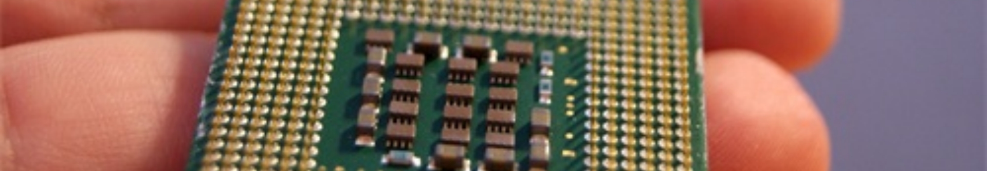
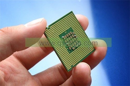
Buried Cavity Package Substrate Manufacturer
Buried Cavity Package Substrate Manufacturer,Buried Cavity Package Substrates are specialized components used in semiconductor packaging, featuring integrated cavities within the substrate structure. These cavities are embedded beneath the surface layers, providing space for housing sensitive components or enhancing thermal management. Buried Cavity Package Substrates offer advantages such as reduced package size, 電気的性能の向上, and enhanced heat dissipation compared to traditional substrates. They are crucial in applications requiring compact and efficient designs, such as high-density integrated circuits, RF/microwave modules, and power electronics. Their innovative design supports advanced packaging techniques and facilitates the integration of multiple functions within a single substrate, meeting the evolving demands of modern electronic devices.
What is a Buried Cavity Package Substrate?
A Buried Cavity Package Substrate refers to a specialized type of substrate used in semiconductor packaging. It involves creating cavities within the substrate material itself, which are then buried under layers of material. These cavities are strategically placed to accommodate various components such as chips, 受動部品, or even other substrates.
The primary purpose of a Buried Cavity Package Substrate is to enable dense integration of components while managing heat dissipation and electrical performance. By embedding components within the substrate, the overall size of the package can be reduced, which is crucial for applications where space is limited, such as in mobile devices or high-performance computing.
Manufacturing Buried Cavity Package Substrates involves precise etching and filling processes to create the cavities and ensure they are properly insulated and protected. The design also considers thermal management and electrical routing to maintain performance and reliability. This substrate type is often chosen for its ability to enhance the functionality and miniaturization of electronic devices.
Buried Cavity Package Substrate Manufacturer
What are the Buried Cavity Package Substrate Design Guidelines?
の設計ガイドライン Buried Cavity Package Substrates typically include several key considerations to ensure optimal performance and manufacturability:
- Cavity Design and Placement: Determine the size, 形, and placement of cavities based on the components to be embedded. Ensure adequate clearance and spacing for neighboring components and signal routing.
- 基板材料選定: Choose substrate materials with suitable thermal conductivity, dielectric properties, and mechanical strength to support the embedded components and maintain reliability under operational conditions.
- レイヤースタックアップ: Define the layer stackup considering the number of signal, 力, and ground planes required. Ensure proper isolation and impedance control for signal integrity.
- Cavity Etching and Filling: Specify the etching technique for creating cavities within the substrate material. Ensure precise control to achieve the desired depth and dimensions. Select appropriate filling materials (例えば。, epoxy resin) to encapsulate the cavities and provide structural integrity.
- サーマルマネジメント:Incorporate thermal vias and thermal pads to enhance heat dissipation from embedded components to the substrate and external heatsinks. Optimize the placement of thermal vias to minimize thermal resistance.
- Electrical Routing: Plan the routing of electrical traces to connect embedded components to the rest of the substrate. Maintain signal integrity by avoiding sharp bends, minimizing crosstalk, and ensuring controlled impedance.
- 機械的な考慮事項: Design the substrate to withstand mechanical stresses during handling and operation. Consider factors such as coefficient of thermal expansion (CTEの) matching with components and assembly materials to prevent solder joint failures.
- Assembly and Testing: Define assembly processes compatible with the substrate design, such as component placement and soldering techniques. Implement testing procedures to verify electrical continuity, 熱性能, and overall reliability.
- Design for Manufacturability (ディエフエム): 設計を最適化して製造を容易に, including considerations for material availability, 費用対効果, and compatibility with fabrication processes (例えば。, エッチング, 積層, filling).
- Reliability and Quality Assurance: Implement measures to ensure long-term reliability, such as adherence to industry standards (例えば。, IPC standards), 信頼性試験 (例えば。, サーマルサイクル, はんだ付け性), and quality control throughout the manufacturing process.
これらの設計ガイドラインに従うことにより、, engineers can develop Buried Cavity Package Substrates that meet performance requirements while facilitating efficient manufacturing and ensuring reliability in electronic applications.
What is the Buried Cavity Package Substrate Fabrication Process?
の製造プロセス Buried Cavity Package Substrates involves several key steps to ensure precise construction and integration of embedded components. Here’s an overview of the typical process:
- 材料の選択: Choose suitable substrate materials, often FR-4 or other high-performance laminates, based on thermal, 電気的な, and mechanical requirements.
- Layer Preparation: Start with the base substrate material, which is laminated into multiple layers according to the design specifications. The layers may include signal, 力, and ground planes.
- Cavity Definition: Use photolithography to define the cavity pattern on the substrate. A photosensitive material is applied, exposed to light, and developed to create a mask for etching.
- エッチング: Employ chemical or laser etching to create cavities in the defined areas. This step requires precision to achieve the desired depth and dimensions for the cavities.
- Cavity Cleaning: Clean the etched cavities to remove any residues and prepare the surfaces for filling. This step is crucial for ensuring adhesion and performance.
- Cavity Filling: Fill the cavities with a suitable material, such as epoxy or other resins. This material supports the embedded components and provides mechanical stability.
- 硬化: Cure the filling material to solidify it, typically involving heat or UV light, depending on the resin used. This step ensures the embedded components are securely held in place.
- Electrical Routing: Implement the necessary electrical routing by drilling vias and etching traces on the surface layers. This allows for connections between embedded components and external circuitry.
- Lamination and Bonding: Laminate additional layers if needed, ensuring proper adhesion and alignment. This step may involve heat and pressure to fuse layers together.
- 最終処理: Complete any additional processes such as surface finishing, applying solder mask, or screen printing for component identification and protection.
- テストと品質保証: Conduct thorough testing to verify electrical performance, サーマルマネジメント, and overall integrity of the substrate. This may include continuity testing, サーマルサイクル, and visual inspections.
次の手順に従います, manufacturers can produce high-quality Buried Cavity Package Substrates that meet the demanding requirements of modern electronic applications.
How do you manufacture a Buried Cavity Package Substrate?
Manufacturing a Buried Cavity Package Substrate involves several detailed steps to ensure precision and functionality. Here’s an overview of the process:
- 材料の選択: Choose a suitable substrate material, typically a high-performance laminate like FR-4 or other advanced materials, based on thermal and electrical properties.
- Layer Preparation: Prepare the base substrate by laminating multiple layers, including signal, ground, and power planes as required by the design.
- Cavity Design: Utilize CAD software to create a design that specifies the size, 形, and placement of cavities. This design is crucial for the subsequent etching process.
- 写真石版: Apply a photosensitive coating (フォトレジスト) on the substrate. Expose it to UV light through a mask that defines the cavity pattern, then develop the photoresist to reveal the areas for etching.
- エッチング: Use chemical etching or laser etching to create cavities in the exposed areas. This process must be carefully controlled to achieve the desired depth and profile.
- 清掃: Thoroughly clean the cavities to remove any residues, ensuring a clean surface for the next steps.
- Cavity Filling: Fill the cavities with a suitable material, such as epoxy or resin, that provides mechanical support for embedded components. This filling can be done using dispensing techniques.
- 硬化: Cure the filling material using heat or UV light to ensure it hardens and securely holds the embedded components in place.
- Electrical Routing: Drill vias and etch traces on the substrate surface to create necessary electrical connections. This involves using techniques like laser drilling and chemical etching.
- Lamination of Additional Layers: If the design requires, laminate additional layers onto the substrate, ensuring proper alignment and bonding through heat and pressure.
- 表面仕上げ: Apply surface finishes such as solder mask or surface treatments to protect the substrate and prepare it for component assembly.
- テストと品質保証: Conduct comprehensive testing to assess electrical performance, thermal characteristics, and structural integrity. This includes continuity tests, サーマルサイクル, and visual inspections.
次の手順に従います, manufacturers can produce high-quality Buried Cavity Package Substrates that meet the needs of advanced electronic applications.
How much should a Buried Cavity Package Substrate cost?
The cost of a Buried Cavity Package Substrate can vary widely based on several factors, 含む:
- 材料: 基板材料の選択 (例えば。, FR-4, 高周波ラミネート) affects pricing. Advanced materials may increase costs.
- Complexity:The complexity of the design, including the number and size of cavities, layer count, and routing requirements, 製造コストに影響を与える可能性があります.
- Volume: Production volume plays a significant role; larger quantities often reduce per-unit costs due to economies of scale.
- 製造技術: The specific processes used (例えば。, エッチング, filling, 硬化) コストに影響を与える可能性があります. More advanced manufacturing methods may be pricier.
- テストと品質管理: Additional costs may arise from testing and quality assurance measures to ensure reliability.
- Supplier: Prices may vary between suppliers based on their capabilities, 場所, and reputation.
As a rough estimate, the cost can range from a few dollars to over $50 per unit, depending on these factors. 正確な価格設定のために, it’s best to consult with manufacturers or suppliers directly, providing them with specific design requirements and volume needs.
What is Buried Cavity Package Substrate base material?
The base material for Buried Cavity Package Substrates typically includes:
- FR-4: A widely used glass-reinforced epoxy laminate, known for its good electrical properties, 機械的強度, そして費用対効果.
- High-Frequency Laminates: Materials such as PTFE (Teflon) or other advanced composites are used for applications requiring low loss and high-frequency performance.
- ポリイミド: Used for applications needing excellent thermal stability and flexibility, often in high-temperature environments.
- セラミック材料: Some substrates may utilize ceramics for their excellent thermal conductivity and electrical insulation properties, suitable for high-performance applications.
The choice of base material depends on the specific application requirements, including thermal management, 電気的性能, そして機械的な完全性.
Which company makes Buried Cavity Package Substrates?
Many companies manufacture Buried Cavity Package Substrates, primarily including electronic manufacturing companies and semiconductor packaging service providers worldwide. These companies typically possess advanced manufacturing technologies and specialized engineering teams to meet diverse customer needs and technical standards.
Buried Cavity Package Substrates are an advanced semiconductor packaging technology that enables higher integration and superior thermal management in electronic devices. These substrates are commonly used in applications requiring high performance and compact size, モバイルデバイスなど, high-performance computing, および通信機器.
The manufacturing of Buried Cavity Package Substrates involves critical technologies and processes, including precise photolithography, chemical etching, selection of filling materials, and curing. Each step requires strict process control and quality assurance to ensure the substrate’s reliability and performance.
Our company is also a manufacturer capable of producing Buried Cavity Package Substrates. We have advanced production equipment and a technical team that can manufacture high-quality Buried Cavity Package Substrates according to customer design requirements and specifications. Our manufacturing process adheres strictly to industry standards, ensuring that every aspect of the product meets the highest quality and performance criteria.
As a manufacturer, we not only focus on technological innovation and production capabilities but also prioritize collaboration with customers to understand their specific needs and provide customized solutions. We offer competitive pricing and excellent customer service, ensuring that clients are satisfied with product quality and delivery times.
If you have further questions about Buried Cavity Package Substrates or are interested in our products, お気軽にお問い合わせください. We are dedicated to providing you with support and service.
は何ですか 7 優れたカスタマーサービスの品質?
Good customer service typically embodies the following seven qualities:
- 応答: Timely responses to customer inquiries and concerns demonstrate that a company values its customers’ time and needs.
- 共感: Understanding and acknowledging customers’ feelings and perspectives helps build rapport and trust.
- Knowledge: Staff should be well-informed about products, services, and policies to provide accurate information and assistance.
- コミュニケーションスキル: クリア, コンサイス, and polite communication helps ensure that customers feel heard and understood.
- Problem-Solving Ability: Being proactive in addressing issues and finding solutions enhances customer satisfaction and loyalty.
- プロ 意識: Maintaining a respectful and courteous demeanor at all times reflects positively on the company.
- フォローアップ: Checking in with customers after their issues have been resolved shows commitment to their satisfaction and fosters long-term relationships.
よくあるご質問(FAQ)
What are the advantages of using Buried Cavity Package Substrates?
Advantages include improved thermal management, 強化された電気的性能, パッケージサイズの縮小, and increased component integration.
What materials are used for Buried Cavity Package Substrates?
一般的な材料にはFR-4が含まれます, 高周波ラミネート (such as PTFE), ポリイミド, とセラミックス, depending on the specific application requirements.
What industries use Buried Cavity Package Substrates?
These substrates are widely used in the electronics industry, particularly in applications like mobile devices, high-performance computing, 自動車用電子機器, and communication systems.
How are Buried Cavity Package Substrates manufactured?
The manufacturing process involves material selection, 写真石版, エッチング, cavity filling, 硬化, electrical routing, and quality testing.
What are the key design considerations for Buried Cavity Package Substrates?
Key considerations include cavity size and placement, サーマルマネジメント, electrical routing, レイヤースタックアップ, と製造可能性.
Can Buried Cavity Package Substrates be customized?
はい, they can be tailored to meet specific customer requirements, including design specifications, material choices, and performance characteristics.
What is the typical lead time for production?
Lead times can vary based on complexity and order volume, but generally range from a few weeks to several months.
What testing is performed on Buried Cavity Package Substrates?
Testing may include electrical continuity, サーマルサイクル, 機械的信頼性, and visual inspections to ensure quality and performance.