
Ajinomoto GZ41R2H Package Substrate Manufacturer
Ajinomoto GZ41R2H Package Substrate Manufacturer,The Ajinomoto GZ41R2H package substrate represents a pinnacle of engineering in electronic packaging. Crafted by Ajinomoto Fine-Techno Co., Ltd., this substrate epitomizes precision and reliability, catering to the demands of the ever-evolving semiconductor industry. Its advanced composition boasts exceptional thermal conductivity, ensuring efficient heat dissipation essential for high-performance electronic devices. With meticulous attention to detail, the substrate offers superior electrical insulation properties, guaranteeing stable and secure connections vital for seamless functionality. Its robust mechanical strength fortifies the structural integrity of electronic assemblies, safeguarding against mechanical stresses and environmental factors. Designed with precision and manufactured with excellence, the Ajinomoto GZ41R2H package substrate stands as a testament to innovation, 確実, and quality craftsmanship, empowering electronic devices with the performance and durability they require in today’s dynamic technological landscape.
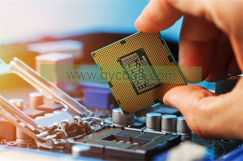
What is Ajinomoto GZ41R2H package substrate?
The Ajinomoto GZ41R2H package substrate is a type of substrate used in semiconductor packaging. It’s manufactured by Ajinomoto Fine-Techno Co., Ltd., a company known for its advanced packaging technologies.
This particular substrate likely belongs to the family of FC-CSP (Flip-Chip Chip-Scale Package) 基板. FC-CSP is a popular packaging technology for integrated circuits, especially in applications where miniaturization, high-density interconnection, and thermal management are critical factors.
The GZ41R2H substrate may offer specific features such as high thermal conductivity, 熱膨張係数が低い (CTEの), そして優秀な電気性能. These characteristics are essential for ensuring reliable operation of semiconductor devices, especially in high-power and high-frequency applications.
The “GZ41R2H” designation likely refers to specific material compositions, 寸法, and design configurations tailored to meet the requirements of particular semiconductor devices or applications.
まとめ, the Ajinomoto GZ41R2H package substrate represents a specialized component in semiconductor packaging, designed to provide optimal performance, 確実, and miniaturization in electronic devices.
Ajinomoto GZ41R2H Package Substrate Manufacturer
What are the Ajinomoto GZ41R2H package substrate Design Guidelines?
Specific design guidelines for the Ajinomoto GZ41R2H package substrate may vary depending on the requirements of the semiconductor device, the application, and the manufacturer’s recommendations. しかし, here are some general design considerations that are commonly applicable:
- サーマルマネジメント: Ensure proper thermal dissipation by optimizing the layout of heat-generating components and providing adequate thermal vias and thermal pads for heat transfer to the PCB (プリント回路基板).
- シグナルインテグリティ: Maintain signal integrity by minimizing signal path lengths, reducing impedance mismatches, and controlling transmission line characteristics such as trace width, spacing, and impedance.
- 電力供給ネットワーク (PDNの): Design an efficient power delivery network with low impedance paths to supply power to the integrated circuit. This includes optimizing power plane layouts, minimizing inductance in power traces, and placing decoupling capacitors strategically.
- Package Size and Layout: Design the package size and layout to meet the size constraints of the overall system while accommodating the required number of I/Os, 信号ルーティング, and thermal considerations.
- Electromagnetic Compatibility (EMCの): Implement EMC best practices to minimize electromagnetic interference (EMIの) and ensure compliance with regulatory standards. This may involve proper shielding, grounding techniques, and layout optimization to reduce radiated emissions and susceptibility to external interference.
- 信頼性に関する考慮事項: Design for reliability by ensuring adequate mechanical support, minimizing stress concentrations, and considering factors such as thermal cycling, 振動, and mechanical shock during operation and handling.
- 製造可能性: 製造可能性を念頭に置いた基板の設計, considering factors such as material compatibility, manufacturing process capabilities, and ease of assembly.
It’s essential to consult the specific design guidelines provided by Ajinomoto Fine-Techno Co., Ltd., or other relevant sources to ensure the optimal performance and reliability of the GZ41R2H package substrate in a given application. かつ, collaboration with semiconductor packaging experts and thorough simulation and testing can help validate the design and identify any potential issues early in the development process.
What is the Ajinomoto GZ41R2H package substrate Fabrication Process?
The fabrication process of the Ajinomoto GZ41R2H package substrate involves several steps, which may include the following:
- 基板材料選定: The fabrication process begins with the selection of appropriate substrate materials based on the desired electrical, 熱の, および機械的特性. These materials may include high-performance laminates, FR-4など, BTの (ビスマレイミドトリアジン), or other advanced materials with enhanced characteristics like low dielectric constant, 高い熱伝導率, and low coefficient of thermal expansion (CTEの).
- 基質調製: The selected substrate materials are prepared by cutting them into the required size and shape according to the design specifications of the package substrate.
- Surface Treatment: Surface treatment processes such as cleaning, roughening, and chemical etching may be employed to prepare the substrate surfaces for subsequent metallization and bonding processes. These treatments ensure proper adhesion and promote uniformity in subsequent layers.
- メタライゼーション: Metallization involves depositing conductive layers onto the substrate surfaces using techniques like sputtering, 蒸発, or electroplating. These metal layers serve as conductive pathways for electrical signals and provide interconnection between the integrated circuit (集積回路) and the external environment.
- Photoresist Application and Patterning: A photoresist material is applied onto the metallized substrate surface and patterned using photolithography techniques. This step defines the layout of circuit traces, ビア, and other features on the substrate.
- エッチング: The substrate is subjected to chemical or plasma etching processes to remove the unwanted portions of the metallized layers, leaving behind the desired circuit patterns and features as defined by the photoresist mask.
- Dielectric Layer Deposition: Insulating dielectric layers are deposited onto the substrate surface to electrically isolate and protect the conductive traces. These dielectric layers may be deposited using techniques such as spin coating, 化学蒸着 (CVD検出器), or plasma-enhanced chemical vapor deposition (PECVD).
- ビアフォーメーション: Vias are formed by drilling or laser ablation through the dielectric layers to establish electrical connections between different conductive layers or to the external environment.
- 表面仕上げ: Surface finishing processes such as solder mask application, surface planarization, and plating may be performed to enhance the substrate’s solderability, flatness, and overall reliability.
- Quality Control and Testing: Throughout the fabrication process, quality control measures are implemented to ensure the integrity, 確実, and performance of the fabricated package substrate. Various testing techniques, 電気試験を含む, 目視検査, and dimensional measurement, are employed to validate the substrate’s compliance with design specifications and industry standards.
- パッケージングと組み立て: Once fabricated, the package substrate is integrated into the semiconductor packaging process, where it serves as the foundation for mounting and interconnecting the integrated circuit (集積回路) die with external components such as lead frames, はんだボール, or interposers.
It’s important to note that the specific details of the fabrication process may vary depending on factors such as the substrate material, design requirements, and manufacturing capabilities of the fabrication facility. Collaboration with experienced substrate manufacturers and adherence to industry best practices are essential for achieving optimal performance and reliability in the final packaged semiconductor device.
How do you manufacture Ajinomoto GZ41R2H package substrate?
Manufacturing the Ajinomoto GZ41R2H package substrate involves several main steps:
- 材料の選択と準備: 第一に, select substrate materials suitable for the GZ41R2H package substrate and prepare them by cutting and shaping according to design requirements.
- Surface Treatment:Clean, roughen, and chemically treat the substrate surfaces to ensure adhesion and uniformity of subsequent layers.
- メタライゼーション:Deposit metal layers on the substrate surfaces using techniques such as sputtering, 蒸発, or electroplating to form conductive pathways and electrical connections.
- フォトリソグラフィーとエッチング: Define circuit patterns using photolithography and remove unwanted metal layer portions through etching to leave desired conductive patterns.
- Dielectric Layer Deposition: Deposit insulating dielectric layers to isolate conductive layers and protect circuit structures.
- ビアフォーメーション: Create vias in the dielectric layers to establish electrical connections between different conductive layers or to external connections.
- 表面仕上げ: Apply surface treatments such as solder mask coating and surface planarization to enhance solderability and overall quality.
- Quality Control and Testing: Perform quality control and testing on the produced package substrate to ensure compliance with design specifications and industry standards.
- Packaging and Integration: Integrate the manufactured package substrate into the semiconductor packaging process, assembling it with other components (such as IC chips, lead frames, and solder balls) to form the final semiconductor device.
These are the general steps involved in manufacturing the Ajinomoto GZ41R2H package substrate. Specific manufacturing details and steps may vary based on manufacturer requirements, テクノロジー, and equipment availability.
How much should an Ajinomoto GZ41R2H package substrate cost?
The cost of an Ajinomoto GZ41R2H package substrate can vary depending on several factors such as:
- Material Cost: The cost of the substrate materials used, including the base substrate material, metallization layers, 誘電体材料, and any surface finishes.
- Manufacturing Complexity: The complexity of the manufacturing process, レイヤー数を含む, the density of features, and the level of precision required, コストに影響を与える可能性があります.
- Volume: 通常, higher volumes lead to lower unit costs due to economies of scale. Larger production runs can spread fixed costs over more units, reducing the cost per unit.
- カスタマイズ: If the substrate requires customization or special features tailored to specific applications or customer requirements, this may increase the cost.
- サプライヤーとの関係: Establishing long-term relationships with suppliers or purchasing in bulk can sometimes lead to discounts or more favorable pricing arrangements.
- 市場の需要: 市況, including supply and demand dynamics, can influence pricing.
- 追加サービス: Additional services such as testing, 品質保証, and technical support may also contribute to the overall cost.
To obtain an accurate cost estimate for an Ajinomoto GZ41R2H package substrate, it’s best to directly contact Ajinomoto Fine-Techno Co., Ltd., or their authorized distributors. They can provide pricing information based on specific requirements, quantities, and any customization needed.
What is Ajinomoto GZ41R2H package substrate base material?
The specific base material used for the Ajinomoto GZ41R2H package substrate isn’t explicitly mentioned in readily available sources. しかし, package substrates like the GZ41R2H typically use advanced materials optimized for high-performance semiconductor packaging applications.
Commonly used base materials for package substrates include:
- FR-4 (難燃 4): FR-4 is a widely used epoxy-based laminate material known for its electrical insulation properties and cost-effectiveness.
- BTの (ビスマレイミドトリアジン): BT is a high-performance thermoset polymer known for its excellent thermal and mechanical properties, making it suitable for demanding applications.
- LCPの (液晶ポリマー): LCP is a high-performance thermoplastic polymer known for its low moisture absorption, 優れた電気的特性, と寸法安定性.
- セラミック基板: セラミック基板, アルミナなど (Al2O3) または窒化アルミニウム (AlNの), are used for applications requiring high thermal conductivity and reliability.
- フレキシブル基板: フレキシブル基板, such as polyimide (円周率), are used in applications requiring flexibility and conformability, such as flexible electronics.
Since the Ajinomoto GZ41R2H package substrate is designed for high-performance applications, it’s likely that it employs advanced base materials optimized for characteristics like thermal management, 電気的性能, と信頼性. For precise information on the base material used in the GZ41R2H substrate, it would be best to refer to documentation provided by Ajinomoto Fine-Techno Co., Ltd., or contact them directly for details.
Which company manufactures Ajinomoto GZ41R2H package substrate?
The Ajinomoto GZ41R2H package substrate is manufactured by Ajinomoto Fine-Techno Co., Ltd., a Japanese company specializing in advanced packaging technologies. They offer various high-performance semiconductor packaging solutions and are renowned for their exceptional technical expertise and high-quality products, positioning them as leaders in the semiconductor industry.
As a high-end packaging technology company, our company also has the capability to produce the Ajinomoto GZ41R2H package substrate. We have advanced production equipment and technology to meet the demand for high-performance and reliable packaging substrates. We prioritize product quality and technological innovation, continuously optimizing our production processes and techniques to ensure that our products meet the most stringent quality standards.
Our production process includes material selection, 表面処理, メタライゼーション, photolithography and etching, dielectric layer deposition, ビアフォーメーション, 表面仕上げ, quality control, とテスト. We employ advanced technologies and strict quality management systems to ensure that each substrate possesses excellent performance and reliability.
We focus on meeting customer demands and offer customized services tailored to their requirements. This includes various material options, different layer counts, sizes, and special process treatments. Our team comprises experienced professionals who can provide technical support and solutions to assist customers in achieving their product design and manufacturing goals.
まとめ, our company has the technical capabilities and production capacity to manufacture the Ajinomoto GZ41R2H package substrate, and we are committed to providing customers with high-quality, high-performance packaging solutions.
は何ですか 7 優れたカスタマーサービスの品質?
Good customer service is characterized by several key qualities that contribute to positive interactions and relationships between businesses and their customers. Here are seven qualities of good customer service:
- 応答: 優れたカスタマーサービスには、お客様からの問い合わせに迅速に対応することが含まれます, 懸念, とリクエスト. This includes acknowledging messages and inquiries in a timely manner and providing timely updates on the status of any ongoing issues or requests.
- 共感: Empathy is essential in understanding and empathizing with customers’ feelings, 懸念, and situations. Good customer service representatives listen actively, show compassion, and strive to understand the customer’s perspective to provide appropriate assistance and support.
- プロ 意識: Good customer service is conducted with professionalism, which involves maintaining a courteous and respectful demeanor at all times, regardless of the customer’s behavior or attitude. Professionalism also entails adhering to company policies and procedures while handling customer inquiries and resolving issues effectively.
- 知識能力:Good customer service representatives possess thorough knowledge about the products or services offered by the company. They are able to answer customer questions accurately, provide helpful recommendations or solutions, and offer relevant information to assist customers in making informed decisions.
- 問題解決スキル: Effective problem-solving skills are crucial in resolving customer issues and complaints efficiently. Good customer service representatives are resourceful, creative, and proactive in finding solutions to customer problems, 困難な状況でも.
- Consistency: Consistency in service delivery is important for building trust and reliability with customers. Good customer service ensures that customers receive consistent levels of service quality and support across all interactions and touchpoints with the company.
- フォローアップとフィードバック: Following up with customers after resolving their issues or completing a transaction demonstrates a commitment to their satisfaction and loyalty. Good customer service includes soliciting feedback from customers to understand their experience, identify areas for improvement, and continuously enhance service quality.
これらの資質を具現化することで、, businesses can cultivate strong relationships with their customers, foster loyalty and satisfaction, and ultimately drive business success.
よくあるご質問(FAQ)
What is the Ajinomoto GZ41R2H package substrate?
The Ajinomoto GZ41R2H package substrate is a specialized substrate used in semiconductor packaging. It is manufactured by Ajinomoto Fine-Techno Co., Ltd. and is designed to meet the high-performance requirements of semiconductor devices.
What are the key features of the Ajinomoto GZ41R2H package substrate?
The specific features of the Ajinomoto GZ41R2H package substrate may vary, but common characteristics include high thermal conductivity, 熱膨張係数が低い (CTEの), そして優秀な電気性能. These features are essential for ensuring the reliability and performance of semiconductor devices.
What applications is the Ajinomoto GZ41R2H package substrate suitable for?
The Ajinomoto GZ41R2H package substrate is suitable for various semiconductor applications, including high-power and high-frequency devices, such as RF (無線周波数) modules, パワーアンプ, and advanced integrated circuits (ICの).
What are the design guidelines for using the Ajinomoto GZ41R2H package substrate?
Design guidelines for the Ajinomoto GZ41R2H package substrate may include considerations for thermal management, シグナルインテグリティ, power delivery network (PDNの) 設計, package size and layout, electromagnetic compatibility (EMCの), 確実, と製造可能性.
How is the Ajinomoto GZ41R2H package substrate fabricated?
The fabrication process of the Ajinomoto GZ41R2H package substrate involves steps such as substrate material selection, 表面処理, メタライゼーション, photolithography and etching, dielectric layer deposition, ビアフォーメーション, 表面仕上げ, quality control, とテスト.
Where can I obtain the Ajinomoto GZ41R2H package substrate?
The Ajinomoto GZ41R2H package substrate is typically available through authorized distributors or directly from Ajinomoto Fine-Techno Co., Ltd. Customers can contact the company or its representatives for inquiries and purchasing information.
Are there any specific considerations for using the Ajinomoto GZ41R2H package substrate in my application?
It’s advisable to consult with semiconductor packaging experts or representatives from Ajinomoto Fine-Techno Co., Ltd. to determine the suitability of the GZ41R2H package substrate for your specific application and to obtain guidance on optimal design and implementation practices.