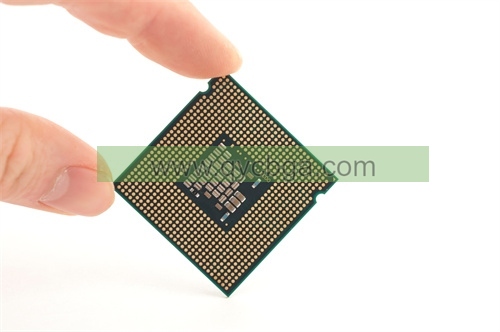
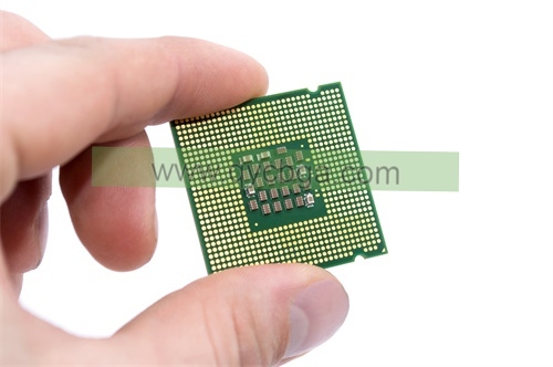
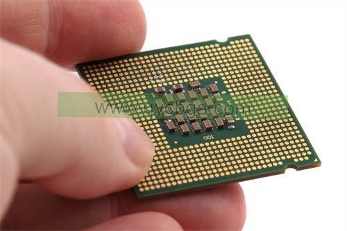
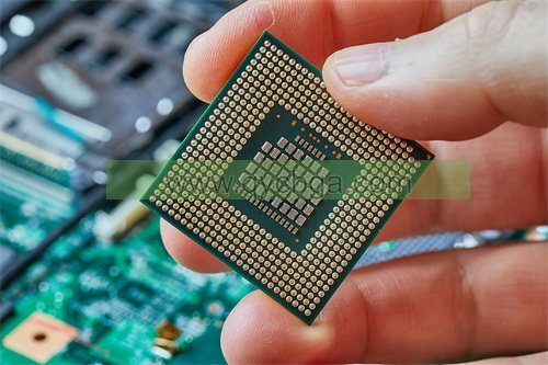
What is SIP Package Substrate?
Hersteller von SIP-Gehäusesubstraten,SIP (System-in-Package) package substrate is a versatile platform designed to integrate multiple semiconductor components into a single, compact module. This substrate supports the stacking and interconnection of various chips, such as processors, Gedächtnis, and passive components, enabling a highly integrated system. SIP substrates offer excellent electrical performance, Thermomanagement, and mechanical stability, often constructed from materials like organic laminates or ceramics. They are ideal for applications requiring miniaturization and high functionality, such as mobile devices, IoT, and wearable electronics. By consolidating multiple functions into one package, SIP package substrates enhance performance, reduce space requirements, and improve overall system reliability.
“SIP” stands for System-in-Package, which refers to a technology where multiple integrated circuits (Ik) or chips are assembled together into a single package. This packaging technique enables the integration of various functions, such as processing, Gedächtnis, and communication, into a compact and efficient form factor.
“Package substrate” in the context of SIP refers to the material or substrate onto which the integrated circuits are mounted and interconnected. It serves as the foundation for the assembly and interconnection of the individual chips within the package.
In the context of semiconductor technology, SIP package substrate plays a crucial role in providing electrical connections between the integrated circuits, managing thermal dissipation, and ensuring mechanical stability of the package. The choice of substrate material and design considerations greatly influence the performance, Zuverlässigkeit, and cost of the SIP package. Substrate materials commonly used in SIP packages include organic substrates (such as FR-4), ceramic substrates, and silicon interposers, among others.
Insgesamt, SIP package substrate technology enables the development of compact, high-performance, and multifunctional electronic systems suitable for a wide range of applications, including consumer electronics, Telekommunikation, automotive, and industrial devices.
SIP Package Substrate design Reference Guide.
The design of SIP (System-in-Package) package substrates is critical for ensuring the performance, Zuverlässigkeit, and manufacturability of integrated circuits (Ik) assembled within a single package. Here is a reference guide detailing key considerations for SIP package substrate design:
- Materialauswahl: Choose substrate materials that meet the electrical, thermisch, and mechanical requirements of the application. Common materials include organic substrates (zum Beispiel., FR-4), ceramic substrates, and silicon interposers. Consider factors such as dielectric constant, thermal conductivity, and coefficient of thermal expansion (CTE).
- Routing and Interconnect Design: Plan and optimize the routing of signal, power, and ground traces to minimize signal degradation, noise, and cross-talk. Use high-density interconnect (HDI) technologies, such as microvias and buried vias, to achieve fine pitch and high interconnect density.
- Signalintegrität (SI) and Power Integrity (PI): Perform SI and PI analysis to ensure signal integrity, Energieverteilung, and electromagnetic compatibility (EMC) compliance. Consider impedance control, signal termination, Platzierung des Entkopplungskondensators, and power delivery network (PDN) design to mitigate SI and PI issues.
- Thermisches Management: Implement effective thermal management techniques to dissipate heat generated by the ICs and ensure reliable operation. Design features such as thermal vias, thermal pads, and heatsinks to enhance heat dissipation and maintain junction temperatures within acceptable limits.
- Package Stacking and Integration: If the SIP involves multiple stacked die or heterogeneous integration, carefully design the package layout and interconnection scheme to minimize parasitic effects, optimize signal paths, and facilitate efficient heat transfer between layers.
- Manufacturability and Reliability: Consider manufacturability aspects such as panelization, fiducial marker placement, Design der Lötstoppmaske, and solder joint reliability. Ensure compliance with industry standards and guidelines for substrate fabrication, Versammlung, and testing.
- Electromagnetic Interference (EMI) Mitigation: Employ EMI mitigation techniques, such as shielding, ground plane design, and signal routing strategies, to minimize electromagnetic emissions and susceptibility to external interference.
- Environmental Considerations: Evaluate the impact of environmental factors, such as temperature fluctuations, Feuchtigkeit, and mechanical stresses, on substrate performance and reliability. Design for robustness and long-term durability under harsh operating conditions.
- Simulation and Prototyping: Utilize simulation tools, such as finite element analysis (FEA), electromagnetic simulation, and thermal analysis software, to model and optimize substrate designs before prototyping. Validate the design through prototyping and testing to verify performance and reliability.
- Documentation and Design Guidelines: Document the SIP package substrate design thoroughly, including schematic diagrams, layout files, design rules, and fabrication specifications. Establish design guidelines and best practices to facilitate collaboration among team members and ensure consistency across projects.
By following these guidelines and considerations, designers can develop optimized SIP package substrate designs that meet the performance, Zuverlässigkeit, and manufacturability requirements of diverse applications in the semiconductor industry.

Hersteller von SIP-Gehäusesubstraten
What are the materials used in SIP Package Substrate?
SIP (System-in-Package) Substrate für Verpackungen can be made from various materials, depending on the specific requirements of the application. Some common materials used in SIP package substrates include:
- Organic Substrates: Organic substrates are typically made of epoxy-based materials reinforced with glass fibers and are commonly known as FR-4 (Flammschutzmittel 4). FR-4 is widely used in PCB (Printed Circuit Board) manufacturing due to its relatively low cost, good electrical insulation properties, and ease of fabrication.
- Ceramic Substrates: Ceramic substrates are made from materials such as alumina (Al2O3) or aluminum nitride (Aln). Ceramic substrates offer excellent thermal conductivity, mechanische Festigkeit, and stability over a wide temperature range. They are often used in high-power applications or environments where high reliability is required.
- Silicon Interposers: Silicon interposers are fabricated using silicon wafers and provide a platform for integrating multiple chips or die within a single package. Silicon interposers offer high interconnect density, low parasitic capacitance, and can incorporate through-silicon vias (TSVs) for vertical interconnects.
- Glass Substrates: Glass substrates, such as borosilicate glass or quartz, are used in certain specialized applications where high thermal stability, low dielectric constant, and excellent optical properties are required.
- Flexible Substrates: Flexible substrates, such as polyimide films, are used in applications requiring flexibility or conformal packaging. Flexible substrates offer advantages in applications such as wearable devices, flexible displays, and bendable electronics.
- Metal Substrates: Metal substrates, wie Aluminium oder Kupfer, are used in applications requiring high thermal conductivity and mechanical stability. Metal substrates are commonly used in high-power LED modules, power electronics, and automotive applications.
- Composite Materials: Composite materials, which combine different materials to achieve specific performance characteristics, may also be used in SIP package substrates. Zum Beispiel, composite substrates may combine organic and ceramic materials to achieve a balance of electrical, thermisch, und mechanische Eigenschaften.
The choice of substrate material depends on factors such as electrical performance, thermal management requirements, Mechanische Stabilität, cost considerations, and the specific needs of the application. Each material has its advantages and limitations, and designers must carefully select the most suitable material based on the requirements of the SIP package design.
How is SIP Package Substrate manufactured?
The manufacturing process for SIP (System-in-Package) Substrate für Verpackungen typically involves several key steps, which may vary depending on the specific substrate material and design requirements. Here is an overview of the general manufacturing process:
- Herstellung von Substraten: The process begins with fabricating the substrate material according to the desired specifications. For organic substrates like FR-4, this involves laminating layers of fiberglass-reinforced epoxy resin and copper foil, followed by drilling holes for vias and through-holes.
- Circuit Patterning: Once the substrate material is prepared, a photolithography process is used to apply a photosensitive material (photoresist) onto the substrate surface. A photomask containing the desired circuit pattern is then aligned and exposed to UV light, transferring the pattern onto the photoresist.
- Etching: Nach der Musterung, the substrate undergoes an etching process to remove the exposed copper material, leaving behind the desired circuit traces. Chemical etchants, such as ferric chloride or ammonium persulfate, are commonly used to dissolve the copper material selectively.
- Plating: In some cases, additional copper plating may be applied to the substrate to increase the thickness of the circuit traces or to add metal layers for multilayer substrates. Electroplating techniques are used to deposit copper onto the substrate surface, followed by a chemical or mechanical process to remove excess copper.
- Oberflächengüte: The substrate’s surface is then coated with a surface finish to protect the copper traces from oxidation and facilitate soldering during assembly. Common surface finishes include hot air solder leveling (HASL), electroless nickel immersion gold (ENIG), immersion silver, or organic solderability preservatives (OSP).
- Drilling and Via Formation: Holes are drilled through the substrate to create vias, which provide electrical connections between different layers in multilayer substrates or between the substrate surface and inner layers. Laser drilling or mechanical drilling processes are used to create these vias, followed by metallization to make electrical connections.
- Assembly and Integration: Once the substrate fabrication is complete, the individual components (such as integrated circuits, Passive Bauelemente, and interconnects) are assembled onto the substrate surface using pick-and-place machines or automated assembly equipment. The components are then bonded to the substrate using various bonding techniques, such as soldering, wire bonding, or flip-chip bonding.
- Testing and Inspection: After assembly, the SIP package substrates undergo testing and inspection to ensure proper functionality, electrical continuity, und Zuverlässigkeit. Various testing methods, including electrical testing, Thermische Zyklen, and X-ray inspection, may be employed to validate the integrity of the assembled substrates.
- Packaging and Encapsulation: Finally, the assembled SIP package substrates may be encapsulated or sealed using epoxy resin or molding compounds to protect the components from environmental factors, mechanical stresses, and moisture ingress.
Insgesamt, the manufacturing process for SIP package substrates involves a combination of precision machining, surface treatment, Versammlung, and testing techniques to produce high-quality substrates suitable for a wide range of electronic applications.
The Application area of SIP Package Substrate
SIP (System-in-Package) package substrates find applications in various industries and electronic devices where compactness, Integration, and high performance are essential. Some common application areas of SIP package substrates include:
- Unterhaltungselektronik: SIP package substrates are widely used in consumer electronics such as smartphones, Tabletten, Wearables, and portable devices. They enable the integration of multiple functions, including processors, Gedächtnis, Sensoren, and wireless connectivity, into compact and power-efficient packages.
- Telecommunications: In telecommunications equipment, SIP package substrates play a crucial role in enabling high-speed data processing, networking, and communication functions. They are used in devices such as routers, Schalter, base stations, and optical transceivers to achieve high performance and reliability.
- Fahrzeugelektronik: SIP package substrates are employed in automotive electronics for various applications, including advanced driver assistance systems (ADAS), Infotainment-Systeme, engine control units (Steuergeräten), and powertrain control modules. They enable the integration of diverse functions while meeting stringent requirements for reliability, temperature tolerance, and durability in automotive environments.
- Industrielle Automatisierung: SIP package substrates are utilized in industrial automation equipment and control systems for tasks such as factory automation, Robotertechnik, process control, and monitoring. They facilitate the integration of sensors, aktoren, microcontrollers, and communication interfaces into compact and rugged packages suitable for harsh industrial environments.
- Medizinprodukte: In the medical industry, SIP package substrates are used in various medical devices and equipment, including diagnostic devices, patient monitoring systems, implantable devices, and medical imaging systems. They enable the integration of sensing, processing, and communication capabilities while meeting regulatory requirements for safety and reliability.
- Luft- und Raumfahrt und Verteidigung: SIP package substrates are employed in aerospace and defense applications for avionics systems, Radarsysteme, electronic warfare systems, and satellite communication systems. They provide high reliability, radiation tolerance, and performance in demanding aerospace and defense environments.
- IoT (Internet of Things): SIP package substrates play a vital role in IoT devices and smart sensors by enabling compact and energy-efficient designs. They are used in applications such as smart home devices, environmental monitoring sensors, wearable health trackers, and industrial IoT solutions to enable connectivity and data processing at the edge.
- Data Centers and Cloud Computing: SIP package substrates are utilized in servers, storage systems, networking equipment, and data center infrastructure for high-performance computing, storage, and networking applications. They enable dense integration of computing, Gedächtnis, and networking components to meet the demands of modern data centers and cloud computing environments.
Insgesamt, SIP package substrates offer versatile solutions for a wide range of applications across industries, enabling compact, integrated, and high-performance electronic systems tailored to specific needs and requirements.
What are the advantages of SIP Package Substrate?
SIP (System-in-Package) package substrates offer several advantages over traditional packaging methods, contributing to their widespread adoption in various electronic applications. Some key advantages of SIP package substrates include:
- Compactness and Integration: SIP package substrates enable the integration of multiple components, such as integrated circuits (Ik), Passive Bauelemente, and interconnects, into a single package. This compact integration reduces the overall footprint of the electronic system, making it suitable for space-constrained applications and enabling miniaturization of devices.
- Improved Electrical Performance: By minimizing the lengths of interconnections between components, SIP package substrates reduce signal propagation delays, impedance mismatches, and signal attenuation. This results in improved electrical performance, including higher signal integrity, faster data transfer rates, and reduced power consumption.
- Enhanced Thermal Management: SIP package substrates allow for more efficient thermal management compared to traditional packaging methods. By integrating heat-generating components closely together and employing thermal vias, thermal pads, and heatsinks, SIP substrates facilitate effective heat dissipation, ensuring reliable operation and prolonging component lifespan.
- Higher Packaging Density: SIP package substrates enable higher packaging densities by utilizing advanced interconnect technologies such as microvias, buried vias, and through-silicon vias (TSVs). This increased packaging density allows for more components to be integrated into a smaller area, enabling the development of high-performance and feature-rich electronic systems.
- Customization and Design Flexibility: SIP package substrates offer greater flexibility in design and customization compared to standard packaging methods. Designers can tailor the substrate layout, interconnect configuration, and component placement to meet specific performance, functionality, and form factor requirements, resulting in optimized solutions for diverse applications.
- Cost Efficiency: Despite the initial investment in design and fabrication, SIP package substrates can offer cost advantages over traditional packaging methods in the long run. The integration of multiple components into a single package reduces assembly and testing costs, lowers material usage, and simplifies supply chain management, leading to overall cost savings.
- Improved Reliability: SIP package substrates can enhance the reliability of electronic systems by reducing the number of interconnects, minimizing the risk of signal degradation, electrical shorts, and mechanical failures. Zusätzlich, SIP substrates facilitate comprehensive testing and inspection processes, ensuring high product quality and reliability.
- Support for Heterogeneous Integration: SIP package substrates support heterogeneous integration by enabling the integration of diverse components, technologies, and materials within a single package. This allows for the integration of advanced functionalities, such as sensors, MEMS devices, RF components, and power management circuits, into a unified system, enabling innovative and versatile electronic products.
Insgesamt, SIP package substrates offer a range of advantages including compactness, improved electrical performance, Thermomanagement, packaging density, design flexibility, cost efficiency, Zuverlässigkeit, and support for heterogeneous integration, making them ideal solutions for a wide range of electronic applications.
How Much Does SIP Package Substrate Cost?
The cost of SIP (System-in-Package) package substrates can vary significantly depending on several factors, einschließlich des Trägermaterials, design complexity, Fertigungsprozesse, component integration, and volume production. Here are some key considerations affecting the cost of SIP package substrates:
- Substratmaterial: The choice of substrate material, such as organic substrates (zum Beispiel., FR-4), ceramic substrates, silicon interposers, or flexible substrates, can influence the overall cost. Organic substrates are typically more cost-effective compared to ceramic or silicon substrates, which may require specialized fabrication processes.
- Komplexität des Designs: The complexity of the SIP package design, einschließlich der Anzahl der Schichten, routing density, component integration, and features such as microvias or buried vias, can impact the manufacturing cost. More complex designs may require additional fabrication steps and higher precision manufacturing processes, leading to increased costs.
- Fertigungsprozesse: The choice of manufacturing processes, such as photolithography, Radierung, plating, Bohrung, Versammlung, and testing, can affect the cost of SIP package substrates. Advanced manufacturing techniques, such as laser drilling, fine-pitch assembly, and advanced surface finishes, may incur higher production costs.
- Component Integration: The integration of multiple components, such as integrated circuits (Ik), Passive Bauelemente, and interconnects, into a single package can affect the overall cost. SIP packages with higher component integration levels may require more advanced assembly techniques and incur higher component costs.
- Volume Production: The production volume or quantity of SIP package substrates can significantly impact the unit cost. Higher volume production typically leads to economies of scale, resulting in lower unit costs due to optimized manufacturing processes, bulk material purchasing, and reduced setup costs.
- Customization and Special Features: Customized SIP package substrates with special features, unique form factors, or specific performance requirements may incur additional development and tooling costs. Specialized features such as embedded passive components, RF shielding, or thermal management solutions can contribute to higher overall costs.
- Supply Chain and Market Factors: Supply chain factors such as material availability, lead times, component pricing, and market demand can influence the cost of SIP package substrates. Fluctuations in material prices, currency exchange rates, and global economic conditions may also impact overall production costs.
Insgesamt, the cost of SIP package substrates can vary widely depending on the specific requirements of the application, design complexity, Fertigungsprozesse, and volume production. It’s essential for designers and manufacturers to carefully consider these factors and balance cost considerations with performance, Zuverlässigkeit, and time-to-market requirements when developing SIP package solutions.
FAQs
What factors influence the cost of SIP package substrates?
The cost of SIP package substrates can be influenced by factors such as substrate material, design complexity, Fertigungsprozesse, component integration, volume production, customization, and supply chain factors.
Which substrate materials are typically more cost-effective for SIP package substrates?
Organic substrates, such as FR-4, are generally more cost-effective compared to ceramic or silicon substrates. Aber, the choice of substrate material depends on specific application requirements.
How does design complexity affect SIP package substrate cost?
More complex designs with higher layer counts, routing density, and special features like microvias or buried vias may require additional manufacturing steps and higher precision processes, leading to increased costs.
What role does manufacturing volume play in SIP package substrate cost?
Higher volume production typically results in economies of scale, leading to lower unit costs due to optimized manufacturing processes, bulk material purchasing, and reduced setup costs.
Are there additional costs associated with customization or special features in SIP package substrates?
Yes, customization or special features such as embedded passive components, RF shielding, or thermal management solutions may incur additional development and tooling costs, impacting overall costs.
How do supply chain and market factors influence SIP package substrate cost?
Factors such as material availability, lead times, component pricing, and market demand can impact SIP package substrate costs. Fluctuations in material prices or global economic conditions may also affect production costs.
Is it possible to reduce SIP package substrate costs without compromising quality?
Yes, cost optimization strategies such as design simplification, Materialauswahl, process optimization, and supply chain management can help reduce SIP package substrate costs while maintaining quality and performance.
 FCBGA Package Substrate Hersteller

