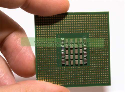
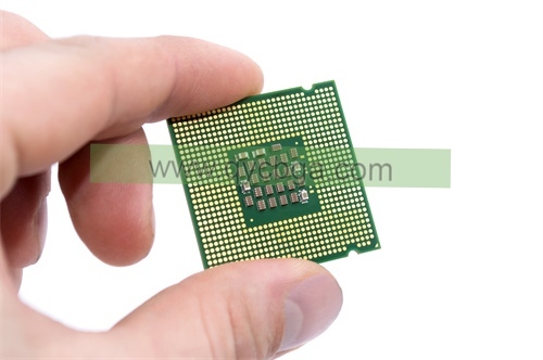
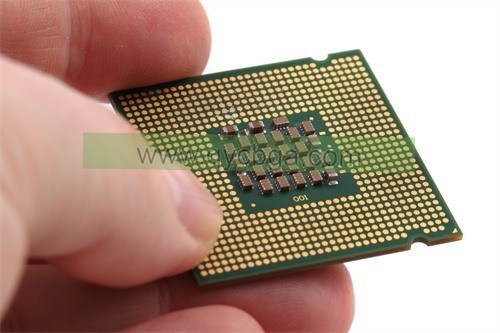
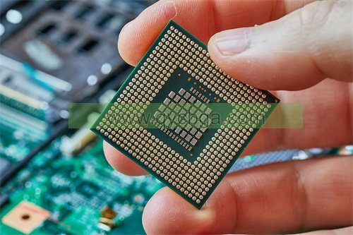
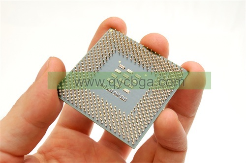
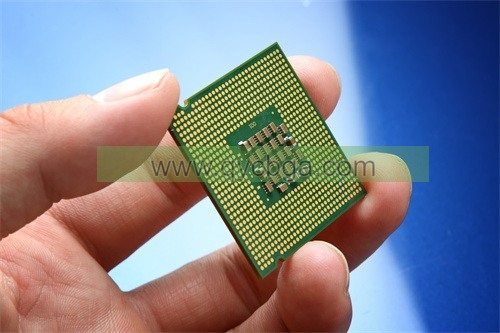
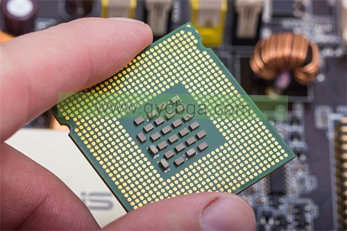
What is PBGA Package Substrate?
ผู้ผลิตพื้นผิวแพ็คเกจ PBGA,PBGA (Plastic Ball Grid Array) package substrate is a widely used packaging technology that facilitates robust electrical connections and enhanced thermal performance for integrated circuits. Constructed from laminate materials, PBGA substrates support a grid of solder balls on the underside, which provide reliable interconnects to the motherboard. This package design offers significant advantages in terms of heat dissipation, reduced electrical resistance, and improved signal integrity, making it highly suitable for high-performance computing and telecommunications equipment. The plastic encapsulation of PBGA substrates also helps in protecting the delicate semiconductor components from environmental and mechanical stresses. Due to its cost-effectiveness and adaptability to various applications, PBGA remains a popular choice among semiconductor package designs.
PBGA stands for Plastic Ball Grid Array. It is a type of integrated circuit packaging used in electronics assembly. The PBGA package substrate refers to the underlying material upon which the integrated circuit (IC) is mounted and interconnected.
The substrate provides a stable base for the IC and serves as the medium for electrical connections between the IC and the rest of the circuitry. It typically consists of layers of insulating material such as fiberglass-reinforced epoxy laminate, with copper traces and vias to facilitate electrical connections.
PBGA packages are known for their compact size, high pin count, and good thermal performance, making them suitable for a wide range of applications including microprocessors, memory chips, and other integrated circuits used in computers, เครื่องใช้ไฟฟ้า, telecommunications, and automotive electronics.
PBGA Package Substrate design Reference Guide.
Designing PBGA package substrates requires careful consideration of various factors such as electrical performance, การจัดการความร้อน, mechanical reliability, และความสามารถในการผลิต. While there may not be a single comprehensive guide covering all aspects of PBGA package substrate design, there are several resources available that provide valuable guidance and reference information. Here are some key points to consider:
- Manufacturer Guidelines: Most substrate manufacturers provide design guidelines and reference materials specific to their products. These guidelines typically include recommendations for layout, การเลือกวัสดุ, via design, routing rules, and other critical aspects of substrate design. Manufacturers may also offer design support services to assist with specific questions or challenges.
- Industry Standards: Organizations such as the IPC (Association Connecting Electronics Industries) publish standards and guidelines related to PCB and substrate design. IPC-7095, เช่น, covers design and assembly considerations for BGAs (Ball Grid Arrays), which includes PBGA packages. These standards often provide valuable insights into best practices and common pitfalls to avoid.
- Simulation and Modeling Tools: Utilize simulation and modeling tools to analyze and optimize substrate designs. Electrical simulation tools can help assess signal integrity, การกระจายพลังงาน, and impedance control, while thermal simulation tools can evaluate heat dissipation and thermal performance. Modeling tools can also aid in predicting mechanical stresses and reliability issues.
- การจัดการความร้อน: Proper thermal management is crucial for PBGA packages, especially for high-power devices such as microprocessors and GPUs. Consider factors such as thermal vias, thermal pad design, heat sink attachment, and overall heat dissipation strategy to ensure adequate cooling and prevent overheating.
- Signal Integrity and Power Distribution: Pay close attention to signal integrity and power distribution within the substrate design. Minimize signal reflections, ครอสทอล์ค, and impedance mismatches by carefully planning signal routing, layer stackup, and via placement. Ensure robust power delivery by optimizing power plane distribution and decoupling capacitor placement.
- Reliability and Manufacturing Considerations: Design substrates with manufacturability and reliability in mind. Consider factors such as solder joint reliability, via plating thickness, pad size, solder mask design, and assembly process compatibility. Collaborate closely with PCB fabrication and assembly partners to ensure that the design meets their requirements and capabilities.
- Documentation and Validation: จัดทําเอกสารการออกแบบพื้นผิวอย่างละเอียด, including layout files, fabrication drawings, material specifications, and assembly instructions. Conduct thorough design reviews and validation tests to verify performance, ความน่าเชื่อถือ, and compliance with specifications.
By following these guidelines and leveraging available resources, designers can develop PBGA package substrates that meet the performance, ความน่าเชื่อถือ, and manufacturability requirements of their specific applications.

ผู้ผลิตพื้นผิวแพ็คเกจ PBGA
What are the materials used in PBGA Package Substrate?
The materials used in PBGA (Plastic Ball Grid Array) package substrates are carefully chosen to provide electrical insulation, mechanical support, and thermal management while also being compatible with the manufacturing processes involved. Common materials found in PBGA package substrates include:
- Substrate Core Material: The core material forms the main body of the substrate and provides structural support. It is typically made of epoxy-based resin reinforced with fiberglass (FR-4) or other materials such as BT (บิสมาเลไมด์ไตรอาซีน) resin for higher performance applications.
- Copper Foil: Copper foil is used to create conductive traces and pads on the substrate layers. It provides electrical connectivity between the IC and other components on the circuit board.
- Dielectric Material: Dielectric material, usually a resin or laminate, is used to insulate the conductive layers and prevent short circuits. It also helps maintain signal integrity by controlling impedance.
- Solder Mask: Solder mask is applied over the conductive traces and pads to protect them from environmental damage and prevent unintended solder connections during assembly. It is typically made of epoxy-based resin.
- เสร็จสิ้นพื้นผิว: Surface finish materials are applied to the exposed copper surfaces to protect them from oxidation and facilitate solder attachment during assembly. Common surface finishes include immersion tin, แช่เงิน, เอนิก (นิกเกิลแช่ทองแบบไม่ใช้ไฟฟ้า), and HASL (การปรับระดับบัดกรีลมร้อน).
- Adhesive: Adhesive materials may be used in multi-layer substrates to bond the layers together. These adhesives must have good thermal and mechanical properties to ensure the integrity of the substrate structure.
- Fillers and Additives: Fillers and additives may be included in the substrate materials to enhance specific properties such as thermal conductivity, ความเสถียรของมิติ, or flame retardancy.
The specific choice of materials depends on factors such as the desired electrical performance, thermal requirements, reliability standards, and cost considerations. Designers must carefully evaluate these factors to select the most suitable materials for a given PBGA package substrate application.
How is PBGA Package Substrate manufactured?
The manufacturing process of PBGA (Plastic Ball Grid Array) package substrates involves several steps, including substrate fabrication, layer buildup, circuit formation, การตกแต่งพื้นผิว, and quality control. นี่คือภาพรวมทั่วไปของกระบวนการผลิต:
- Substrate Fabrication: The process begins with the fabrication of the substrate core material. This typically involves laminating layers of epoxy-based resin with fiberglass reinforcement (FR-4) or other materials. The substrate core material is then cured to form solid panels of the desired thickness.
- Layer Buildup: Multiple layers of conductive copper foil and dielectric material are then bonded together to create a multi-layered substrate. This process involves laminating thin sheets of copper foil onto both sides of the substrate core material, with layers of dielectric material sandwiched in between.
- Circuit Formation: The conductive copper foil is patterned and etched to create the desired circuitry, including traces, pads, and vias. This is typically done using a combination of photolithography, แกะ สลัก, and plating processes. Solder mask is applied over the conductive traces and pads to protect them and define areas for solder attachment.
- การตกแต่งพื้นผิว: Surface finish materials are applied to the exposed copper surfaces to protect them from oxidation and facilitate solder attachment during assembly. Common surface finishes include immersion tin, แช่เงิน, เอนิก (นิกเกิลแช่ทองแบบไม่ใช้ไฟฟ้า), and HASL (การปรับระดับบัดกรีลมร้อน).
- Quality Control: ตลอดกระบวนการผลิต, various quality control measures are implemented to ensure the integrity and reliability of the PBGA package substrates. ซึ่งอาจรวมถึงการตรวจสอบด้วยสายตา, การทดสอบทางไฟฟ้า, dimensional measurements, and adherence to industry standards and specifications.
- Assembly Compatibility: ในที่สุด, the PBGA package substrates are designed to be compatible with the assembly processes used to attach the ICs and other components. This may involve incorporating features such as solder mask defined (SMD) pads, solder mask openings for vias, and appropriate surface finishes for solder attachment.
ทั้งหมด, the manufacturing process of PBGA package substrates requires precision and attention to detail to produce substrates that meet the performance, ความน่าเชื่อถือ, and manufacturability requirements of modern electronic devices. Collaboration between substrate manufacturers, PCB designers, and assembly partners is often necessary to ensure successful production and integration into electronic assemblies.
The Application area of PBGA Package Substrate
PBGA (Plastic Ball Grid Array) package substrates find application in a wide range of electronic devices across various industries due to their compact size, high pin count, good thermal performance, และความน่าเชื่อถือ. พื้นที่การใช้งานทั่วไปบางส่วน ได้แก่:
- เครื่องใช้ไฟฟ้า: PBGA package substrates are extensively used in consumer electronics such as smartphones, แท็บ เล็ต, แล็ป ท็อป, กล้องดิจิตอล, and gaming consoles. They provide the necessary connectivity and performance for microprocessors, memory chips, and other integrated circuits in these devices.
- Computing and Networking: In computing and networking equipment such as servers, เรา เตอร์, สวิตช์, and storage devices, PBGA package substrates play a crucial role in providing high-speed data processing and communication capabilities. They are used for microprocessors, application-specific integrated circuits (ASICs), network processors, and memory modules.
- Telecommunications: PBGA package substrates are used in telecommunications infrastructure equipment such as base stations, optical networking devices, and communication servers. They enable efficient data transmission, signal processing, and network management functions.
- อิเล็กทรอนิกส์ยานยนต์: In automotive applications, PBGA package substrates are employed in engine control units (ECU), infotainment systems, navigation systems, advanced driver assistance systems (ADAS), and other electronic modules. They help manage vehicle functions, enhance safety, and provide entertainment and connectivity features.
- Industrial Electronics: PBGA package substrates are utilized in various industrial applications such as factory automation, การควบคุมกระบวนการ, วิทยาการหุ่นยนต์, เครื่องมือวัด, and power management systems. They enable precise control, monitoring, and automation of industrial processes and equipment.
- Medical Devices: In medical electronics, PBGA package substrates are found in diagnostic equipment, imaging systems, patient monitoring devices, and medical implants. They support the processing, storage, and transmission of medical data and facilitate accurate diagnosis and treatment.
- Aerospace and Defense: In aerospace and defense applications, PBGA package substrates are used in avionics systems, ระบบเรดาร์, communication systems, navigation systems, and electronic warfare systems. They provide the reliability, การแสดง, and ruggedness required for operation in harsh environments.
ทั้งหมด, PBGA package substrates play a vital role in enabling the functionality, การแสดง, and connectivity of modern electronic devices across a diverse range of applications and industries.
What are the advantages of PBGA Package Substrate?
PBGA (Plastic Ball Grid Array) package substrates offer several advantages that make them popular in various electronic applications. ข้อได้เปรียบที่สําคัญบางประการ ได้แก่:
- Compact Size: PBGA packages have a high pin density and a compact footprint, allowing designers to achieve higher levels of integration and miniaturization in electronic devices. This is particularly advantageous in applications where space is limited, such as mobile devices and portable electronics.
- High Pin Count: PBGA packages can accommodate a large number of pins, providing ample connectivity for complex integrated circuits such as microprocessors, ASICs, and memory modules. This high pin count makes PBGA packages suitable for high-performance computing and networking applications.
- Good Thermal Performance: PBGA packages typically feature a thermally enhanced design with a large thermal pad underneath the package. This allows for efficient heat dissipation, which is crucial for maintaining the reliability and performance of high-power electronic components, especially in applications with demanding thermal requirements.
- Mechanical Robustness: PBGA packages are mechanically robust and resistant to mechanical stresses such as shock and vibration. The solder balls provide a reliable interconnection between the package and the PCB, ensuring robustness in harsh operating environments such as automotive, อวกาศ, and industrial applications.
- Enhanced Electrical Performance: The short interconnect lengths and controlled impedance characteristics of PBGA packages help minimize signal degradation and improve electrical performance, including signal integrity and high-speed data transmission. This makes PBGA packages suitable for applications requiring high-frequency operation and low noise.
- Ease of Assembly: PBGA packages are relatively easy to assemble compared to other types of packages such as quad flat packages (QFP) or leaded chip carriers (LCC). The solder balls on the bottom of the package simplify the soldering process, leading to faster and more cost-effective assembly.
- Compatibility with Advanced Technologies: PBGA packages are compatible with advanced packaging technologies such as flip-chip bonding, system-in-package (SiP), and 3D integration, enabling further performance improvements and integration capabilities in future electronic designs.
ทั้งหมด, PBGA package substrates offer a compelling combination of performance, ความน่าเชื่อถือ, และความสามารถในการผลิต, making them a preferred choice for a wide range of electronic applications across industries.
How Much Does PBGA Package Substrate Cost?
The cost of PBGA (Plastic Ball Grid Array) package substrates can vary significantly depending on various factors such as the size of the substrate, the complexity of the circuitry, จํานวนชั้น, การเลือกใช้วัสดุ, and the manufacturing processes involved. โดยทั่วไป, the cost of PBGA package substrates is influenced by the following factors:
- Size and Complexity: Larger substrates with more complex circuitry will typically cost more to manufacture due to the increased material and manufacturing complexity required.
- Number of Layers: Multi-layer substrates with more layers will incur higher manufacturing costs compared to single-layer or double-layer substrates due to the additional materials and processing steps involved.
- การเลือกวัสดุ: The choice of substrate materials, such as the type of core material, copper foil thickness, and surface finish, can impact the overall cost. High-performance materials or specialized features may increase the cost.
- Manufacturing Processes: The specific manufacturing processes used to fabricate the substrate, such as lamination, แกะ สลัก, plating, and surface finishing, อาจส่งผลต่อต้นทุน. Advanced processes or customization may incur higher costs.
- Volume and Economy of Scale: Higher volumes of production typically result in lower per-unit costs due to economies of scale. Conversely, low-volume or prototype runs may have higher per-unit costs.
- ซัพพลายเออร์และที่ตั้ง: The choice of substrate supplier and manufacturing location can also influence the cost. Different suppliers may offer varying pricing structures, and manufacturing costs may vary based on factors such as labor costs, regulatory requirements, and infrastructure.
It’s important to note that PBGA package substrates are often just one component of the overall cost of an electronic device. Other factors such as the cost of the integrated circuits, สภา, การทดสอบ, บรรจุ ภัณฑ์, and overhead expenses also contribute to the total cost of the final product.
For specific pricing information, individuals or companies would need to consult with substrate manufacturers or suppliers directly, as costs can vary widely depending on the requirements of the project and the negotiated terms.
FAQs about PBGA Package Substrate
What is a PBGA package substrate?
A PBGA package substrate is a type of integrated circuit packaging used to mount and interconnect electronic components, such as microprocessors and memory chips, onto a printed circuit board (PCB). It consists of a plastic encapsulated body with an array of solder balls on the bottom for electrical connections.
What are the advantages of PBGA package substrates?
Some advantages of PBGA package substrates include compact size, high pin count, good thermal performance, mechanical robustness, enhanced electrical performance, ease of assembly, and compatibility with advanced packaging technologies.
What materials are used in PBGA package substrates?
Common materials used in PBGA package substrates include epoxy-based resin for the substrate core, copper foil for conductive traces, dielectric material for insulation, solder mask for protection, and surface finish materials such as immersion tin or gold for solder attachment.
How are PBGA package substrates manufactured?
The manufacturing process of PBGA package substrates involves steps such as substrate fabrication, layer buildup, circuit formation, การตกแต่งพื้นผิว, and quality control. This process includes laminating substrate layers, patterning and etching conductive traces, applying surface finishes, and ensuring product quality.
What are the applications of PBGA package substrates?
PBGA package substrates find application in various electronic devices across industries such as consumer electronics, computing and networking, telecommunications, อุปกรณ์อิเล็กทรอนิกส์ยานยนต์, industrial electronics, อุปกรณ์ทางการแพทย์, and aerospace and defense.
How much do PBGA package substrates cost?
The cost of PBGA package substrates can vary depending on factors such as size, complexity, จํานวนชั้น, การเลือกวัสดุ, กระบวนการผลิต, volume, ผู้ให้, and location. Pricing information is typically obtained by consulting with substrate manufacturers or suppliers directly.
Where can I find more information about PBGA package substrates?
More information about PBGA package substrates can be found through datasheets, application notes, technical articles, industry publications, and consultation with substrate manufacturers or suppliers. นอกจากนี้, online forums and communities may provide insights and discussions related to PBGA package substrates.
 ผู้ผลิตพื้นผิวแพ็คเกจ FCBGA

