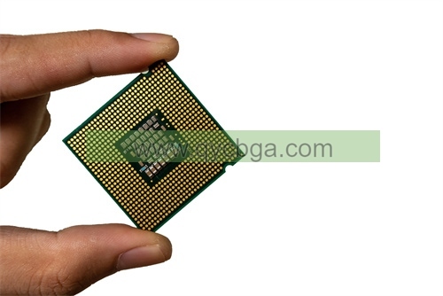
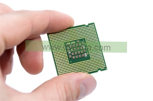
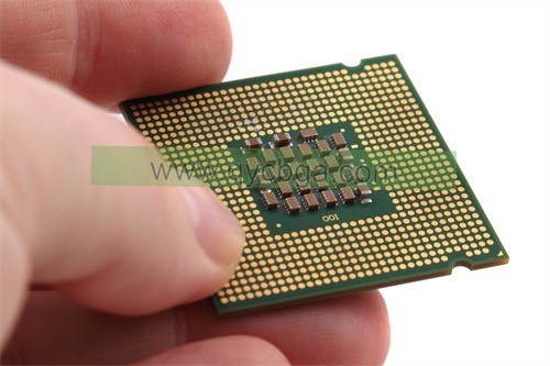
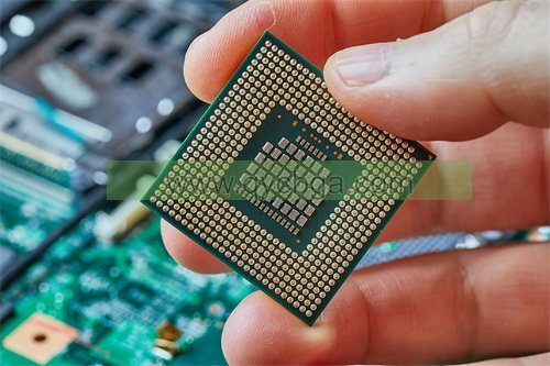
What is Cavity Package Substrate?
Cavity Package Substrate Manufacturer,Cavity package substrate is a specialized material designed for housing and protecting sensitive electronic components. It features a recessed cavity that accommodates chips and other devices, providing robust mechanical support and enhanced thermal management. This design minimizes the thermal and mechanical stresses on the components, ensuring reliable performance in high-frequency and high-power applications. Cavity package substrates are often made from materials with excellent thermal and electrical properties, such as ceramics or advanced composites. They are widely used in telecommunications, aerospace, and military industries, where durability and precise performance are critical. These substrates enable compact and efficient packaging solutions for complex electronic systems.
In a cavity package substrate, the cavity provides a recessed area for the die to be mounted, allowing for better protection and heat dissipation. This configuration can offer several advantages, including improved thermal performance, better electrical characteristics, and potentially smaller overall package size.
Cavity package substrates are commonly used in various semiconductor applications where thermal management and performance are critical, such as high-power RF (radio frequency) devices, power amplifiers, and power management ICs (integrated circuits). They are designed to efficiently dissipate heat generated by the semiconductor device, which is essential for maintaining device reliability and performance.

Cavity Package Substrate Manufacturer
Cavity Package Substrate (CPS) design Reference Guide.
The design of Cavity Package Substrates (CPS) is crucial in ensuring optimal performance, reliability, and thermal management of semiconductor devices. A comprehensive reference guide for CPS design should encompass various aspects, including substrate materials, cavity geometry, electrical considerations, thermal management, and manufacturing processes. Here’s an expanded guide covering these aspects:
- Substrate Materials: CPS substrates are typically made from high thermal conductivity materials such as ceramics (e.g., alumina or aluminum nitride) or specialized organic substrates. The choice of material depends on factors like thermal performance requirements, cost, and compatibility with assembly processes.
- Cavity Geometry: The design of the cavity within the substrate is critical for accommodating the semiconductor die. Factors such as the size, shape, depth, and alignment of the cavity impact electrical performance, mechanical stability, and thermal dissipation.
- Electrical Considerations: CPS design must consider electrical characteristics such as signal integrity, power distribution, and impedance matching. Proper routing of electrical traces, vias, and bond pads is essential to minimize signal loss and maintain reliable electrical connections.
- Thermal Management: Effective heat dissipation is paramount in CPS design to prevent overheating and ensure device reliability. Strategies include optimizing the thermal conductivity of substrate materials, designing thermal vias for heat dissipation, incorporating heat spreaders or heat sinks, and implementing thermal interface materials for efficient heat transfer.
- Manufacturing Processes: The reference guide should cover manufacturing techniques such as substrate fabrication, cavity formation (e.g., laser drilling or mechanical milling), die attachment methods (e.g., soldering or adhesive bonding), wire bonding or flip-chip assembly, encapsulation, and finishing processes (e.g., solder mask application or surface finish).
- Design Guidelines: Provide guidelines for layout design, including die placement, routing of signal and power traces, placement of decoupling capacitors, and clearance requirements for electrical and thermal isolation.
- Reliability Considerations: Address reliability concerns such as mechanical stress, thermal cycling, moisture ingress, and solder joint integrity. Design features like underfill encapsulation, corner fillets, and proper material selection can enhance the reliability of CPS assemblies.
- Testing and Quality Control: Discuss testing methodologies and quality control measures to ensure the integrity and performance of CPS devices. This may include electrical testing, thermal characterization, visual inspection, and reliability testing (e.g., temperature cycling, mechanical shock, and vibration testing).
- Packaging Standards and Specifications: Reference relevant industry standards and specifications governing CPS design, materials, assembly processes, and reliability testing to ensure compliance and interoperability with existing systems.
- Case Studies and Examples: Include real-world case studies and examples illustrating successful CPS designs, highlighting best practices, challenges encountered, and lessons learned.
By addressing these key aspects comprehensively, the CPS design reference guide serves as a valuable resource for engineers and designers involved in the development of semiconductor devices with cavity package substrates, facilitating optimized performance, reliability, and manufacturability.
What are the materials used in Cavity Package Substrate (CPS)?
Cavity Package Substrates (CPS) utilize various materials to provide structural support, electrical connectivity, and thermal management for semiconductor devices. The choice of materials depends on factors such as performance requirements, cost considerations, and manufacturing processes. Common materials used in CPS include:
- Substrate Material: The substrate serves as the structural foundation for the package. Common substrate materials include ceramics such as alumina (Al2O3) or aluminum nitride (AlN), as well as organic substrates like FR-4 (a type of epoxy-based laminate). These materials offer different properties in terms of thermal conductivity, coefficient of thermal expansion (CTE), and electrical insulation.
- Dielectric Layers: Dielectric materials are used to insulate conductive traces and vias on the substrate to prevent electrical shorts. Materials like silicon dioxide (SiO2) or polyimide-based films are commonly used for dielectric layers due to their excellent electrical insulation properties and compatibility with semiconductor processes.
- Conductive Traces and Vias: Copper (Cu) is the most common material used for conductive traces and vias due to its excellent electrical conductivity. Copper traces are patterned on the substrate to provide interconnections between the semiconductor die and external circuitry.
- Solder Mask: Solder mask materials are applied over the substrate to protect conductive traces from environmental factors and prevent unintended solder bridges during assembly. Epoxy-based solder mask materials are commonly used due to their excellent adhesion properties and resistance to soldering processes.
- Solder Balls/Pads: In flip-chip or ball grid array (BGA) configurations, solder balls or pads are used to establish electrical connections between the semiconductor die and the substrate. These solder balls are typically made of tin-lead (SnPb) or lead-free alloys such as tin-silver-copper (SnAgCu) or tin-silver (SnAg).
- Underfill Materials: Underfill materials are used to encapsulate the space between the semiconductor die and the substrate, providing mechanical support and improving reliability by reducing stress on solder joints. Epoxy-based underfill materials are commonly used due to their excellent adhesion and thermal expansion properties.
- Heat Spreaders/Heat Sinks: In applications requiring enhanced thermal management, additional heat spreaders or heat sinks may be attached to the substrate to dissipate heat generated by the semiconductor device. These heat spreaders are typically made of materials with high thermal conductivity, such as copper or aluminum.
By carefully selecting and optimizing the materials used in CPS design, manufacturers can achieve the desired performance, reliability, and cost-effectiveness for a wide range of semiconductor packaging applications.
How is Cavity Package Substrate (CPS) manufactured?
The manufacturing process for Cavity Package Substrates (CPS) involves several steps to fabricate the substrate, assemble semiconductor components, and encapsulate the package. Below is an overview of the typical manufacturing process for CPS:
- Substrate Fabrication:
– Substrate material selection: Choose the appropriate substrate material based on the desired electrical, thermal, and mechanical properties.
– Substrate preparation: Cut the substrate material into the desired size and shape.
– Surface preparation: Clean the substrate surface to remove contaminants and ensure proper adhesion of subsequent layers.
- Cavity Formation:
– Cavity design: Design the cavity layout according to the size and shape of the semiconductor die.
– Cavity creation: Use processes such as milling, laser ablation, or chemical etching to create cavities in the substrate.
– Surface planarization: Smoothen the cavity surfaces to ensure uniform die attachment and improve reliability.
- Layer Deposition:
– Dielectric layer deposition: Apply dielectric materials onto the substrate surface to insulate conductive traces and vias.
– Conductive trace formation: Deposit and pattern conductive materials (e.g., copper) onto the substrate to create interconnects and bonding pads.
- Die Attachment:
– Die placement: Position the semiconductor die within the cavities on the substrate.
– Die bonding: Use techniques such as soldering or conductive adhesive bonding to attach the die to the substrate.
- Interconnection:
– Wire bonding or flip-chip bonding: Establish electrical connections between the semiconductor die and the substrate using wire bonding or flip-chip bonding techniques.
– Solder ball attachment (if applicable): Attach solder balls or pads to establish connections between the substrate and external circuitry.
- Encapsulation:
– Underfill application: Dispense underfill materials around the semiconductor die to provide mechanical support and protect solder joints.
– Encapsulant deposition: Apply encapsulant materials over the substrate to encapsulate the semiconductor components and provide environmental protection.
– Curing: Cure the underfill and encapsulant materials using heat or UV radiation to ensure proper adhesion and mechanical strength.
- Post-processing:
– Cleaning: Remove any residues or contaminants from the substrate surface.
– Testing: Perform electrical and mechanical tests to verify the functionality and reliability of the CPS.
– Marking and labeling: Mark the CPS with identifying information such as part numbers, date codes, and logos.
- Packaging and Shipping:
– Package assembly: Place the CPS into protective packaging materials such as trays or tape-and-reel for shipment.
– Quality control: Conduct final inspections to ensure that the CPS meets all quality standards and specifications.
By following these manufacturing steps, manufacturers can produce Cavity Package Substrates that meet the performance, reliability, and cost requirements of various semiconductor applications.
The Application area of Cavity Package Substrate (CPS)
Cavity Package Substrates (CPS) find applications in various industries and technologies where advanced semiconductor packaging is required. Some of the key application areas include:
- High-Frequency RF (Radio Frequency) Devices: CPS technology is commonly used in high-frequency RF devices such as RF power amplifiers, RF transceivers, and RF switches. The cavity design helps in reducing parasitic capacitance and inductance, improving signal integrity and performance at high frequencies.
- Power Electronics: CPS is utilized in power semiconductor devices like power amplifiers, voltage regulators, and power management ICs (Integrated Circuits). The cavity structure enhances thermal dissipation, allowing for efficient heat management in high-power applications.
- Wireless Communication Systems: CPS is employed in wireless communication systems including cellular base stations, satellite communication equipment, and wireless routers. The enhanced thermal management and electrical performance of CPS make it suitable for high-reliability communication infrastructure.
- Automotive Electronics: In automotive electronics, CPS is used in applications such as radar systems, vehicle-to-vehicle (V2V) communication modules, and advanced driver-assistance systems (ADAS). The rugged design and thermal performance of CPS are well-suited for the harsh operating conditions in automotive environments.
- Aerospace and Defense: CPS technology is applied in aerospace and defense systems such as radar systems, avionics, electronic warfare systems, and satellite payloads. The compact size, high reliability, and thermal management capabilities of CPS are advantageous for space-constrained and mission-critical applications.
- Medical Devices: In medical electronics, CPS is used in equipment such as MRI machines, ultrasound devices, and implantable medical devices. The high-density interconnects and thermal performance of CPS contribute to miniaturization and reliability in medical device applications.
- Industrial Automation: CPS finds applications in industrial automation systems including motor drives, programmable logic controllers (PLCs), and robotics. The efficient thermal management and compact size of CPS support the demanding requirements of industrial environments.
- Consumer Electronics: CPS technology is increasingly being adopted in consumer electronics products such as smartphones, tablets, and wearable devices. The compact size and thermal efficiency of CPS contribute to the design of thinner and more power-efficient consumer electronics devices.
Overall, the versatility, reliability, and performance characteristics of Cavity Package Substrates make them suitable for a wide range of applications across industries where advanced semiconductor packaging solutions are required.
What are the advantages of Cavity Package Substrate (CPS)?
Cavity Package Substrates (CPS) offer several advantages over traditional semiconductor packaging technologies, making them suitable for various applications. Some of the key advantages of CPS include:
- Enhanced Thermal Management: The cavity design of CPS facilitates efficient heat dissipation from the semiconductor die to the substrate, allowing for better thermal management. This helps in reducing operating temperatures and improving the reliability and longevity of semiconductor devices, especially in high-power applications.
- Reduced Parasitic Capacitance and Inductance: The cavity structure of CPS minimizes parasitic capacitance and inductance compared to surface-mounted packages. This results in improved electrical performance, higher signal integrity, and reduced signal loss, making CPS suitable for high-frequency RF and high-speed digital applications.
- Miniaturization: CPS enables the integration of semiconductor components into compact and space-efficient packages. The cavity design allows for the embedding of semiconductor dies within the substrate, reducing the overall footprint of the package. This is particularly beneficial for applications where space constraints are critical, such as portable electronics and IoT devices.
- Improved Reliability: The structural support provided by the cavity substrate and the use of advanced materials contribute to the enhanced reliability of CPS. The reduced mechanical stress on solder joints, improved thermal stability, and protection from environmental factors help in increasing the lifespan and durability of semiconductor devices.
- High-Density Interconnects: CPS allows for high-density interconnects with fine pitch traces and vias, enabling the integration of complex semiconductor circuits and functionalities. This facilitates the implementation of advanced semiconductor technologies such as system-on-chip (SoC) and multi-chip modules (MCM), leading to improved performance and functionality.
- Customization and Flexibility: CPS technology offers flexibility in design and customization to meet specific application requirements. Manufacturers can tailor the substrate material, cavity dimensions, interconnect layout, and package configuration according to the needs of the application, allowing for optimized performance and cost-effectiveness.
- Compatibility with Advanced Packaging Techniques: CPS is compatible with various advanced packaging techniques such as flip-chip bonding, chip-on-board (COB) assembly, and 3D integration. This compatibility enables the integration of multiple semiconductor dies, sensors, and passive components within a single package, enhancing functionality and performance.
- Cost-Effectiveness: Despite offering advanced features and performance benefits, CPS can be cost-effective compared to other advanced packaging technologies. The use of standard substrate materials, scalable manufacturing processes, and optimized designs contribute to cost efficiency, making CPS viable for a wide range of applications and market segments.
Overall, the advantages of Cavity Package Substrates make them an attractive choice for semiconductor packaging in applications where thermal management, electrical performance, miniaturization, reliability, and customization are critical factors.
How Much Does Cavity Package Substrate (CPS) Cost?
The cost of Cavity Package Substrates (CPS) can vary significantly depending on various factors such as the complexity of the design, substrate material, manufacturing processes, volume production, and supplier pricing. However, CPS typically tends to be more expensive compared to standard surface-mount packages due to its advanced features and manufacturing requirements. Here are some factors influencing the cost of CPS:
- Substrate Material: The choice of substrate material can significantly impact the cost of CPS. Ceramic substrates such as alumina (Al2O3) or aluminum nitride (AlN) are generally more expensive compared to organic substrates like FR-4 due to their superior thermal and electrical properties.
- Manufacturing Processes: The manufacturing processes involved in CPS production, including cavity formation, die attachment, interconnect formation, encapsulation, and testing, contribute to the overall cost. Advanced processes such as laser ablation, flip-chip bonding, and underfill dispensing may incur higher production costs compared to traditional assembly methods.
- Design Complexity: The complexity of the CPS design, including the number of cavities, interconnects, and layers, can influence manufacturing costs. Highly customized designs with intricate features may require additional processing steps and materials, resulting in higher costs.
- Volume Production: Economies of scale play a significant role in determining the cost of CPS. Larger production volumes typically result in lower per-unit costs due to optimized manufacturing processes, bulk material purchasing, and reduced setup costs per unit.
- Supplier Pricing: The pricing policies of CPS suppliers and contract manufacturers also affect the overall cost. Factors such as supplier reputation, quality standards, lead times, and supply chain dynamics can influence pricing negotiations.
- Additional Features: Additional features such as integrated heat spreaders, advanced thermal management solutions, and specialized coatings may increase the cost of CPS.
Given these factors, it is challenging to provide a specific cost estimate for CPS without considering the specific requirements of the application, volume production quantities, and supplier agreements. Generally, CPS is considered a premium packaging solution suitable for applications where performance, reliability, and customization are paramount, and the cost is justified by the value it provides in terms of improved functionality and reliability. Organizations interested in adopting CPS should engage with suppliers to obtain detailed cost estimates based on their specific needs and volume requirements.
FAQs
What is a Cavity Package Substrate (CPS)?
A CPS is a type of semiconductor packaging technology where the semiconductor die is mounted within a cavity in the substrate, rather than being mounted directly onto the substrate’s surface. This design enhances thermal management and electrical performance.
What are the advantages of using CPS?
CPS offers advantages such as enhanced thermal management, reduced parasitic capacitance and inductance, miniaturization, improved reliability, high-density interconnects, customization flexibility, compatibility with advanced packaging techniques, and cost-effectiveness.
What applications are suitable for CPS?
CPS is used in various industries and technologies, including high-frequency RF devices, power electronics, wireless communication systems, automotive electronics, aerospace and defense, medical devices, industrial automation, and consumer electronics.
What materials are used in CPS?
Materials commonly used in CPS include substrate materials like ceramics (e.g., alumina, aluminum nitride) or organic substrates (e.g., FR-4), dielectric layers (e.g., silicon dioxide, polyimide), conductive traces (e.g., copper), solder mask materials, solder balls/pads, underfill materials, and heat spreaders/heat sinks.
How is CPS manufactured?
The manufacturing process for CPS involves steps such as substrate fabrication, cavity formation, layer deposition, die attachment, interconnection, encapsulation, post-processing (cleaning, testing, marking), and packaging/shipping.
What factors influence the cost of CPS?
Factors affecting the cost of CPS include substrate material, manufacturing processes, design complexity, volume production, supplier pricing, and additional features such as integrated heat spreaders or advanced thermal management solutions.
What are some considerations when selecting CPS for a specific application?
When selecting CPS for a particular application, factors to consider include performance requirements (thermal, electrical), reliability considerations, space constraints, customization needs, cost constraints, and compatibility with existing systems or technologies.
Are there any challenges associated with CPS?
While CPS offers many benefits, challenges such as design complexity, manufacturing process optimization, thermal management optimization, and cost considerations may need to be addressed depending on the specific application requirements.
 FCBGA Package Substrate manufacturer

