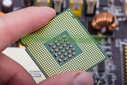
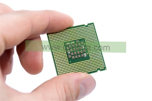
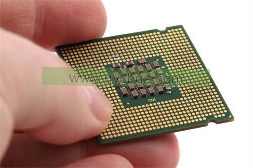
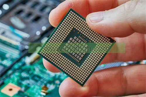
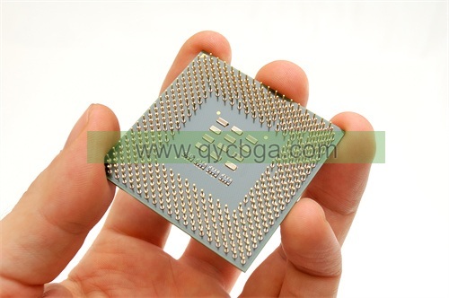
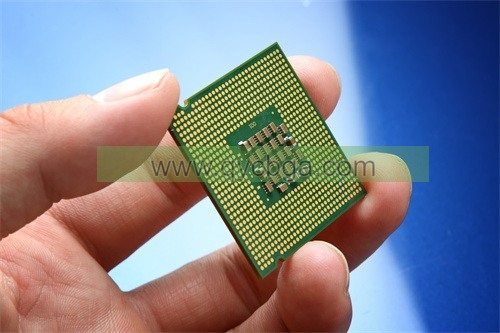
What is BGA/IC Package Substrate?
BGA/IC 패키지 기판 제조업체,증권사 (Ball Grid Array) / IC package substrate is a key component in modern electronics packaging technology, designed to support high-density interconnections. This substrate utilizes a grid of solder balls on its underside, which connect directly to the circuit board, facilitating improved electrical performance and superior thermal management compared to older packaging methods. BGA substrates are renowned for their ability to reduce inductance and increase the speed of signal transmission, making them ideal for applications requiring high-speed computing, such as servers, GPU, and high-performance microprocessors. Made from materials like ceramic or high-performance organic laminates, BGA substrates offer robust mechanical stability and are tailored to withstand the thermal cycles associated with device operation, ensuring long-term reliability and efficiency.

BGA/IC 패키지 기판 제조업체
BGA/IC Package Substrate design Reference Guide.
A reference guide for 증권사 (Ball Grid Array) and IC (Integrated Circuit) package substrate design would typically cover various aspects of designing substrates for these types of packages. Here’s a general outline of what such a guide might include:
- Introduction to BGA and IC Packages: This section provides an overview of BGA and IC packages, including their applications, advantages, and common usage scenarios.
- Substrate Materials: Discuss the different types of substrate materials commonly used in BGA and IC package designs, such as FR-4, FR-5, 구체의, and ceramic. Explain the properties of each material and considerations for selecting the appropriate one based on the specific requirements of the application.
- Design Guidelines: 기판 레이아웃 설계를 위한 지침 제공, including trace routing, 비아 플레이스먼트, and component placement. Discuss best practices for minimizing signal integrity issues, such as crosstalk and signal distortion.
- Signal Integrity and Power Integrity: Provide an overview of signal integrity and power integrity considerations in BGA and IC package substrate design. Discuss techniques for managing high-speed signals, reducing noise, and ensuring reliable power distribution.
- 열 관리: Cover techniques for managing thermal issues in BGA and IC package designs, such as thermal vias, 방열판, 및 열 패드. Discuss considerations for dissipating heat effectively to prevent overheating and maintain component reliability.
- 제조 고려 사항: Explain considerations for manufacturing BGA and IC package substrates, including fabrication processes, layer stackup design, and design for manufacturability (DFM) guidelines.
- Testing and Reliability: Discuss testing methodologies and reliability considerations for BGA and IC package substrates, including electrical testing, 열 순환, and mechanical reliability testing.
- 사례 연구 및 사례: Provide real-world examples and case studies of BGA and IC package substrate designs, highlighting successful implementations and lessons learned.
- Resources and Tools: Include references to additional resources, such as industry standards, design tools, and simulation software, to aid in BGA and IC package substrate design.
By covering these topics comprehensively, a reference guide for BGA and IC package substrate design can serve as a valuable resource for engineers and designers working in the field of semiconductor packaging.
What are the materials used in BGA/IC Package Substrate?
증권사 (Ball Grid Array) and IC (Integrated Circuit) package substrates can be made from various materials, each with its own properties and advantages. Some of the common materials used in BGA and IC package substrates include:
- 프렌-4 (난연성 4): FR-4 is a widely used substrate material in PCB (Printed Circuit Board) 제작. It’s a type of epoxy-based laminate composed of woven fiberglass cloth impregnated with epoxy resin. FR-4 substrates offer good electrical insulation properties, 기계적 강도, 그리고 비용 효율성, making them suitable for many applications.
- 구체의: Polyimide substrates, often referred to as “flexible circuits” or “flex PCBs,” are made of a flexible polymer material. Polyimide substrates are lightweight, thin, and flexible, making them ideal for applications requiring flexibility or space constraints. They also offer good thermal stability and chemical resistance.
- 질그릇의: Ceramic substrates are composed of ceramic materials such as alumina (알2O3) or aluminum nitride (알엔). Ceramic substrates offer excellent thermal conductivity, 기계적 강도, and dimensional stability, making them suitable for high-power and high-frequency applications. They are often used in applications where thermal management is critical.
- Rigid-Flex: Rigid-flex substrates combine rigid and flexible materials into a single substrate structure. They offer the benefits of both rigid and flexible substrates, allowing for complex PCB designs that require both flexibility and rigidity. Rigid-flex substrates are commonly used in applications such as aerospace, 의료 기기, and portable electronics.
- 메탈 코어: Metal core substrates, also known as metal-core PCBs (MCPCBs) or thermal substrates, have a metal core layer typically made of aluminum or copper, 단열재 층 사이에 끼워져 있습니다.. Metal core substrates offer excellent thermal conductivity, making them suitable for applications requiring efficient heat dissipation, such as LED lighting and power electronics.
- Liquid Crystal Polymer (증권 시세 표시기): LCP substrates are composed of a thermoplastic polymer material with high thermal stability, excellent dimensional stability, and low moisture absorption. LCP substrates are often used in high-frequency and high-speed applications due to their low dielectric constant and low loss tangent.
The choice of substrate material depends on various factors such as the specific application requirements, performance criteria, 비용 고려 사항, and manufacturing capabilities. Designers often select the most appropriate substrate material based on a careful evaluation of these factors.
How is BGA/IC Package Substrate manufactured?
The manufacturing process for BGA (Ball Grid Array) and IC (Integrated Circuit) 패키지 기판에는 여러 단계가 포함됩니다., 기판 제조 포함, 금속, 집회, 및 테스트. 다음은 일반적인 제조 공정에 대한 개요입니다:
- 기판 제작:
– Material Preparation: The chosen substrate material (예), 프렌-4, 구체의, 질그릇의) is prepared in the form of sheets or panels.
– Layer Stackup: Multiple layers of substrate material may be laminated together to form a multilayer substrate. Each layer may have copper foil bonded to it for subsequent circuit patterning.
– Drilling and Plating: Holes for vias and through-holes are drilled into the substrate material, and then the holes are plated with conductive material to establish electrical connections between layers.
- 금속:
– 회로 패터닝: A layer of copper is deposited onto the substrate surface using techniques like additive or subtractive processes. This copper layer will form the conductive traces and pads of the substrate.
– Photolithography: A photoresist is applied to the copper layer, and a photomask with the desired circuit pattern is used to expose the photoresist to UV light. The exposed areas are then developed, leaving behind the patterned photoresist.
– 에칭: The exposed copper areas not protected by the photoresist are etched away using an etchant solution, leaving behind the desired copper traces and pads.
- 표면 마감:
– 표면 처리: The substrate surface is cleaned and prepared for the application of surface finish materials.
– Application of Surface Finish: Common surface finish options for BGA and IC package substrates include electroless nickel immersion gold (수수께끼), immersion silver, 유기 납땜성 방부제 (증권 시세 표시기), and solder mask.
- Assembly:
– Component Placement: 표면 실장 구성 요소, IC 포함, passive components, and other devices, 픽 앤 플레이스 기계를 사용하여 기판에 배치됩니다..
– 리플로 솔더링: The assembled substrate undergoes reflow soldering, where solder paste is applied to the component pads, and then the substrate is heated to melt the solder, forming solder joints between the components and the substrate.
- 테스트 및 검사:
– 전기 테스트: Various electrical tests are performed to ensure the functionality and integrity of the substrate, including continuity testing, insulation resistance testing, and high-voltage testing.
– Optical Inspection: Visual inspection is conducted to check for defects such as solder bridges, misaligned components, and solder voids.
– X-ray 검사: X-ray imaging may be used to inspect the integrity of solder joints and internal connections, especially for complex BGA packages.
- 포장 및 배송:
– Once the substrates pass quality control and testing, they are packaged according to customer requirements and shipped to the assembly facility where the ICs will be mounted onto them.
제조 공정 전반에 걸쳐, quality control measures are implemented to ensure that the substrates meet the required specifications for functionality, 신뢰도, and performance.
The Application area of BGA/IC Package Substrate
증권사 (Ball Grid Array) and IC (Integrated Circuit) package substrates find applications across a wide range of industries and electronic devices due to their versatility, 신뢰도, and compact form factor. Some of the common application areas for BGA/IC package substrates include:
- 소비자 가전제품: BGA/IC package substrates are extensively used in consumer electronic devices such as smartphones, 정제, 노트북, 디지털 카메라, gaming consoles, and smart TVs. These substrates enable the miniaturization of electronic components and support high-density interconnects, allowing for compact and lightweight designs.
- 통신: BGA/IC package substrates are essential components in telecommunications equipment, including routers, 스위치, 기지국, and communication modules. They provide the necessary interconnectivity and signal processing capabilities required for high-speed data transmission and network communication.
- 자동차 전자 장치: BGA/IC package substrates are employed in various automotive electronic systems, including engine control units (ECU (에큐)), 인포테인먼트 시스템, 첨단 운전자 보조 시스템 (ADAS (장애인 대한)), 및 차량 네트워킹 모듈. These substrates withstand harsh operating conditions such as temperature fluctuations, 진동, 그리고 수분, ensuring reliable performance in automotive applications.
- 산업용 전자 제품: BGA/IC package substrates play a vital role in industrial automation equipment, instrumentation devices, 제어 시스템, and robotics. They facilitate the integration of complex electronic components and sensors, enabling precise control and monitoring in industrial environments.
- 의료 기기: BGA/IC package substrates are utilized in medical devices and equipment such as diagnostic instruments, 환자 모니터링 시스템, medical imaging devices, and implantable devices. These substrates meet stringent requirements for reliability, accuracy, and safety in medical applications.
- 항공우주 및 방위 산업: BGA/IC package substrates are deployed in aerospace and defense systems, including avionics, 레이더 시스템, communication satellites, missile guidance systems, and unmanned aerial vehicles (UAVs). They withstand extreme temperatures, radiation, and mechanical stress encountered in aerospace and defense environments.
- Networking and Data Centers: BGA/IC package substrates are integral components in networking equipment, data center servers, storage systems, and high-performance computing (HPC) clusters. They support high-speed data processing, routing, and storage, contributing to the efficiency and scalability of networking infrastructure.
- Energy Systems: BGA/IC package substrates are used in energy generation, distribution, and storage systems, including solar inverters, wind turbines, battery management systems, and smart grid devices. They enable efficient energy conversion, 모니터링, and control in renewable energy and power management applications.
전반적, BGA/IC package substrates play a crucial role in enabling the functionality, 공연, and reliability of electronic devices across various industries and applications.
What are the advantages of BGA/IC Package Substrate?
증권사 (Ball Grid Array) and IC (Integrated Circuit) package substrates offer several advantages over traditional packaging methods, contributing to their widespread adoption in various electronic devices and applications. Some of the key advantages of BGA/IC package substrates include:
- High Density Packaging: BGA substrates allow for high-density integration of electronic components and interconnects, enabling the design of compact and miniaturized electronic devices. This is particularly beneficial in applications where space is limited or where a high component count is required.
- Improved Electrical Performance: BGA/IC package substrates typically feature shorter electrical traces and reduced parasitic capacitance and inductance compared to traditional packaging methods. This results in improved signal integrity, reduced electromagnetic interference (이엠아이), and enhanced electrical performance, especially at high frequencies.
- 향상된 열 관리: BGA substrates are well-suited for efficient thermal management due to their compact size and the ability to dissipate heat through the entire substrate surface. This helps to mitigate thermal issues, such as overheating of electronic components, and improves the reliability and longevity of the device.
- Mechanical Stability and Reliability: BGA/IC package substrates provide excellent mechanical stability and reliability due to the soldered connections between the package and the substrate. The solder balls or bumps used in BGA packages distribute mechanical stress more evenly compared to traditional leaded packages, reducing the risk of solder joint fatigue and failure.
- Simplified Assembly Process: BGA packages facilitate automated assembly processes, such as pick-and-place and reflow soldering, resulting in higher throughput and lower manufacturing costs. The absence of leads or pins simplifies the assembly process and reduces the likelihood of misalignment or solder bridging during soldering.
- Improved Electrical Contact: BGA packages feature an array of solder balls or bumps distributed across the underside of the package, providing a large number of electrical contact points with the substrate. This enhances electrical connectivity and reduces the risk of electrical discontinuities or open circuits, leading to improved device reliability.
- Resistance to Environmental Factors: BGA/IC package substrates are typically more resistant to environmental factors such as moisture, dust, and vibration compared to traditional packaging methods. This makes them suitable for use in harsh operating environments, including automotive, 항공 우주, and industrial applications.
- Advanced Technologies와의 호환성: BGA/IC package substrates are compatible with advanced technologies such as flip-chip bonding, system-in-package (SiP), 및 3D 통합, allowing for further miniaturization and integration of electronic systems.
전반적, the advantages of BGA/IC package substrates make them a preferred choice for designers and manufacturers seeking to optimize performance, 신뢰도, and manufacturability in electronic devices.
How Much Does BGA/IC Package Substrate Cost?
The cost of BGA (Ball Grid Array) and IC (Integrated Circuit) 패키지 기판은 여러 요인에 따라 크게 달라질 수 있습니다, 기판 재료를 포함하여, 크기, 복잡성, 양, and customization requirements. 또한, market conditions, supplier pricing, and technology advancements can also impact the cost.
Here are some factors that influence the cost of BGA/IC package substrates:
- 기판 재료: Different substrate materials, such as FR-4, 구체의, 질그릇의, and metal core, have varying costs associated with their fabrication and processing. Ceramic substrates, 예를 들어, tend to be more expensive due to their higher thermal conductivity and performance characteristics.
- Complexity and Layer Count: The complexity and layer count of the substrate affect the manufacturing process complexity, material usage, and production time, thus influencing the overall cost. Multilayer substrates with intricate designs and high-density interconnects typically incur higher manufacturing costs.
- Surface Finish and Features: Surface finish options, such as ENIG (무전해 니켈 침지 금), immersion silver, 증권 시세 표시기 (유기 납땜성 방부제), and special features like blind and buried vias, 임피던스 제어, and HDI (High-Density Interconnect) technology, can add to the cost of the substrate.
- Quantity and Volume Discounts: Larger quantities of BGA/IC package substrates usually qualify for volume discounts from manufacturers or suppliers. Bulk orders can reduce the per-unit cost significantly compared to smaller quantities.
- 사용자 정의 및 특별 요구 사항: Customization requirements, such as specific designs, materials, or features tailored to the application’s needs, may increase the cost of the substrates. Special requirements for testing, qualification, and compliance certification can also impact the overall cost.
- Supplier and Market Dynamics: Market conditions, supplier pricing strategies, and competition among substrate manufacturers can influence the cost of BGA/IC package substrates. Prices may vary between different suppliers and regions based on factors like supply chain logistics, 인건비, 및 환율.
As a result of these factors, it’s challenging to provide a specific cost estimate for BGA/IC package substrates without considering the individual project requirements and sourcing options. Designers and manufacturers typically obtain quotes from multiple suppliers based on their specifications and volume requirements to determine the most cost-effective solution for their applications.
FAQs about BGA/IC Package Substrate
What is a BGA package substrate?
A BGA package substrate is a type of substrate used in semiconductor packaging, specifically designed to accommodate Ball Grid Array packages. It provides mechanical support and electrical interconnects between the IC and the printed circuit board (폴리염화비페).
What are the advantages of using BGA package substrates?
BGA package substrates offer advantages such as high density packaging, improved electrical performance, 향상된 열 관리, mechanical stability, simplified assembly processes, 환경 요인에 대한 내성.
What materials are commonly used in BGA package substrates?
Common materials used in BGA package substrates include FR-4, 구체의, 질그릇의, 금속 코어, and liquid crystal polymer (증권 시세 표시기), each offering different properties and performance characteristics.
How are BGA package substrates manufactured?
The manufacturing process for BGA package substrates involves substrate fabrication, 금속, 표면 마감 응용 프로그램, component assembly (구성 요소 조립), 테스트, and inspection. It includes processes such as layer stackup, circuit patterning, drilling and plating, 솔더 마스크 적용, component placement, 그리고 썰물 납땜.
What are the key considerations for designing BGA package substrates?
Key considerations for designing BGA package substrates include substrate material selection, layer stackup design, 추적 라우팅, 비아 플레이스먼트, 열 관리, 신호 무결성, power integrity, 제조 가능성, and reliability.
What applications are BGA package substrates used in?
BGA package substrates find applications across various industries and electronic devices, 소비자 가전 제품 포함, 통신, 자동차 전자 장치, 산업 자동화, 의료 기기, aerospace and defense, 네트워킹, and energy systems.
What factors affect the cost of BGA package substrates?
Factors affecting the cost of BGA package substrates include substrate material, complexity and layer count, surface finish and features, quantity and volume discounts, customization and special requirements, and supplier and market dynamics.
Where can I find suppliers of BGA package substrates?
Suppliers of BGA package substrates can be found through online directories, industry trade shows, electronic component distributors, and semiconductor packaging companies. It’s advisable to obtain quotes from multiple suppliers and evaluate their capabilities and offerings.
 FCBGA 패키지 기판 제조업체

