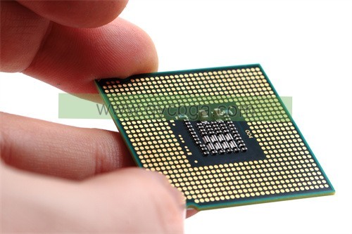
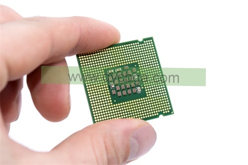
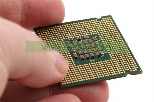
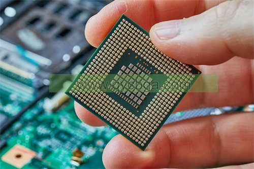
What is ABF(아지노모토) Package Substrate?
증권 시세 표시기(아지노모토) 패키지 기판 제조업체,증권 시세 표시기 (Ajinomoto Build-up Film) package substrate is a cutting-edge material used in semiconductor packaging, known for its exceptional electrical properties and reliability. This substrate employs a build-up film technology, enabling the creation of multiple layers of conductive traces and insulating materials in a compact form factor. ABF substrates offer high thermal conductivity, excellent signal integrity, and mechanical stability, making them ideal for high-speed and high-density applications. Commonly utilized in advanced semiconductor packages like FCBGA and WLP, ABF package substrates ensure reliable performance and durability in diverse electronic devices, from smartphones to data centers, where space efficiency and reliability are critical.
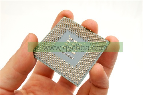
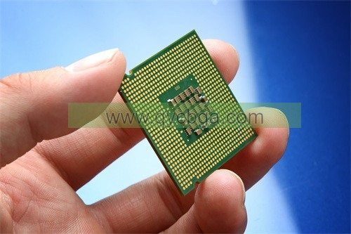
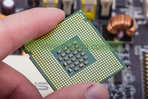
FCBGA stands for “Flip-Chip Ball Grid Array.” It’s a type of integrated circuit packaging technology used in the semiconductor industry. FCBGA 포장에서, 실리콘 다이 (실제 집적 회로) is flipped upside down and mounted directly onto the substrate (usually a ceramic or organic material).
The substrate contains a grid array of solder balls, which serve as the electrical connections between the die and the circuit board it’s mounted on. This type of packaging offers several advantages, including better electrical performance, improved thermal management, and a smaller footprint compared to traditional packaging methods.
The substrate itself is a key component of the FCBGA package. It provides mechanical support for the die and facilitates the electrical connections between the die and the rest of the system. The substrate material can vary depending on the specific requirements of the application, but it’s typically a high-performance material capable of handling the electrical and thermal demands of the integrated circuit.

증권 시세 표시기(아지노모토) 패키지 기판 제조업체
증권 시세 표시기(아지노모토) Package Substrate design Reference Guide.
The ABF (Ajinomoto Buildup Film) 기판 is a type of packaging substrate used in semiconductor manufacturing. It’s a build-up substrate made of layers of insulating material with embedded copper traces to create the electrical connections between the various components of an integrated circuit. Ajinomoto is a company known for its development and production of ABF substrates.
A reference guide for ABF package substrate design would typically include information on:
- Substrate Material Specifications: Details about the composition and properties of the ABF substrate material, including electrical, thermal, and mechanical characteristics.
- Design Guidelines: Guidelines for designing the layout of the substrate, including rules for trace routing, 비아 플레이스먼트, pad sizes, 및 레이어 스택업.
- Signal Integrity Considerations: Information on minimizing signal degradation and electromagnetic interference (이엠아이) through proper substrate design, including controlled impedance routing and power distribution network design.
- 열 관리: Strategies for managing heat dissipation within the package, such as thermal vias and heat spreaders, to ensure proper functioning of the integrated circuit.
- Package Size and Dimensions: Recommendations for determining the appropriate size and dimensions of the substrate based on the specific requirements of the application.
- Reliability Guidelines: Guidelines for ensuring the long-term reliability of the package, including considerations for solder joint integrity, 기계적 스트레스, 및 환경적 요인.
- 제조 및 조립 지침: Recommendations for manufacturing processes, such as substrate fabrication and assembly techniques, to ensure high-yield production and quality.
- Electrical Test Guidelines: Guidelines for testing the electrical performance of the substrate, including test methodologies and criteria for acceptable performance.
These are some of the key aspects that would typically be covered in a reference guide for ABF package substrate design. It serves as a comprehensive resource for engineers and designers involved in the development of integrated circuits using ABF substrates.
What are the materials used in ABF(아지노모토) Package Substrate?
The ABF (Ajinomoto Buildup Film) package substrate is typically composed of several layers of materials, each serving specific functions in the construction and performance of the substrate. While exact compositions may vary depending on specific requirements and applications, here are the typical materials used in ABF package substrates:
- Buildup Layers: The core of the ABF substrate consists of multiple buildup layers, which are thin films of insulating material. These layers are typically made of a polymer material such as polyimide or epoxy resin. These layers provide electrical insulation between the copper traces and facilitate the creation of multilayer interconnect structures.
- Copper Traces: Embedded within the buildup layers are copper traces, which serve as conductive pathways for electrical signals. These traces are patterned using lithographic processes and are typically plated onto the insulating layers. Copper provides good electrical conductivity and is suitable for high-speed signal transmission.
- Barrier Layers: 경우에 따라, barrier layers may be included within the buildup structure to prevent diffusion of copper ions into the insulating material, which could degrade its electrical properties over time. Barrier layers are typically made of materials such as titanium or tantalum.
- 솔더 마스크: The topmost layer of the substrate is often a solder mask, which is a protective coating applied over the copper traces to prevent oxidation and facilitate soldering during assembly. Solder mask materials are typically epoxy-based or polyimide-based and are applied using a screen printing process.
- 표면 마감: The exposed copper pads on the substrate’s surface may be coated with a surface finish to enhance solderability and prevent oxidation. 일반적인 표면 마감에는 무전해 니켈 침지 금이 포함됩니다. (수수께끼), 유기 납땜성 방부제 (증권 시세 표시기), and immersion tin or silver.
- Adhesive Layers: Adhesive layers may be used in ABF substrates to bond the buildup layers together and to attach the substrate to other components in the package assembly. Adhesive materials are typically epoxy-based and are applied as thin films between the buildup layers during fabrication.
These are the primary materials used in the construction of ABF package substrates. The specific composition and layering scheme may vary depending on factors such as performance requirements, 제조 공정, and cost considerations.
How is ABF(아지노모토) Package Substrate manufactured?
The manufacturing process for ABF (Ajinomoto Build-up Film) package substrates involves several steps to create high-density interconnect (HDI) substrates suitable for semiconductor packaging. While specific details may vary depending on the manufacturer and the exact requirements of the application, the general process typically includes the following key stages:
- 기판 준비: The process begins with the preparation of the base substrate material, typically a polyimide film. The film may undergo surface treatment to enhance adhesion and promote uniformity.
- 박판: Multiple layers of dielectric material, usually in the form of dry films or liquid resins, are laminated onto the base substrate. These layers serve as the insulation between conductive traces and define the substrate’s electrical and mechanical properties.
- 회로 패터닝: Copper foil is bonded to the dielectric layers using an adhesive, and then the desired circuit patterns are created through processes such as photolithography and etching. Photolithography involves applying a photoresist layer onto the copper foil, exposing it to UV light through a photomask with the desired circuit pattern, and then developing the resist to define the pattern. Etching removes the exposed copper, leaving behind the desired traces.
- 비아 포메이션: Vias, which are small holes drilled or formed through the substrate layers, are created to establish electrical connections between different layers of the substrate. This can be achieved using laser drilling, mechanical drilling, or via punching processes.
- Build-Up Process: Additional dielectric layers and conductive traces are sequentially added using a build-up process, which involves repeating the lamination, patterning, and via formation steps as necessary to achieve the desired number of layers and interconnect density.
- 표면 마무리: The substrate’s surface is typically coated with a solder mask to define solderable areas and protect the underlying copper traces. Surface finishes such as immersion gold or electroless nickel immersion gold (수수께끼) may also be applied to improve solderability and corrosion resistance.
- Final Inspection and Testing: The completed ABF package substrates undergo rigorous inspection and testing to ensure they meet quality and performance standards. This may include visual inspection, 전기 테스트, and reliability testing to assess factors such as thermal cycling, solder joint reliability, and dimensional accuracy.
By following these manufacturing steps, ABF package substrate manufacturers can produce high-quality substrates tailored to the specific requirements of semiconductor packaging applications, including those demanding high-density interconnects, fine-pitch traces, and excellent electrical performance.
The Application area of ABF(아지노모토) Package Substrate
증권 시세 표시기 (Ajinomoto Build-up Film) package substrates find applications in various sectors of the semiconductor industry, particularly in advanced packaging technologies where space constraints, high signal density, and superior electrical performance are critical factors. 몇 가지 일반적인 응용 분야는 다음과 같습니다:
- 모바일 장치: ABF substrates are widely used in the packaging of mobile devices such as smartphones, 정제, and wearables. Their thin profile, lightweight nature, and ability to accommodate high-density interconnects make them ideal for compact and portable electronics.
- 소비자 가전제품: Beyond mobile devices, ABF substrates are also employed in a range of consumer electronics products including digital cameras, gaming consoles, smart home devices, 및 휴대용 미디어 플레이어. These applications benefit from ABF substrates’ ability to support miniaturization and high-speed data transfer.
- Networking and Telecommunications: ABF package substrates play a crucial role in networking and telecommunications equipment such as routers, 스위치, 기지국, and optical transceivers. These applications demand high-performance interconnect solutions to support data communication and networking protocols.
- 자동차 전자 장치: In the automotive industry, ABF substrates are used in advanced driver assistance systems (ADAS (장애인 대한)), 인포테인먼트 시스템, engine control units (ECU (에큐)), 및 기타 전자 부품. They offer reliability, thermal stability, and the ability to withstand harsh operating conditions.
- Industrial Applications: ABF substrates are also employed in various industrial applications such as industrial automation, 로봇공학, 제어 시스템, and instrumentation. Their ability to handle high-speed data transmission and operate in demanding environments makes them well-suited for industrial applications.
- 의료 기기: In the medical sector, ABF substrates are utilized in medical imaging equipment, patient monitoring devices, diagnostic tools, 및 이식형 의료 기기. They offer reliability, miniaturization, and high-density interconnects critical for medical device design.
- 항공우주 및 방위 산업: ABF package substrates are used in aerospace and defense applications including avionics, 레이더 시스템, communication equipment, 그리고 미사일 유도 시스템. They provide the reliability, 공연, and ruggedness required for aerospace and defense electronics.
전반적, ABF package substrates are versatile solutions that cater to a wide range of applications across industries where compact size, 고성능, and reliability are paramount. Their ability to meet stringent requirements for miniaturization, high-speed data transfer, and thermal management makes them indispensable in the semiconductor packaging landscape.
What are the advantages of ABF(아지노모토) Package Substrate?
증권 시세 표시기 (Ajinomoto Build-up Film) package substrates offer several advantages that make them attractive options for semiconductor packaging applications. 주요 이점 중 일부는 다음과 같습니다:
- High-Density Interconnects: ABF substrates enable the creation of high-density interconnects, allowing for more compact and miniaturized electronic packages. This is particularly beneficial in applications where space constraints are critical, such as mobile devices and wearable electronics.
- Fine-Pitch Traces: ABF substrates support the creation of fine-pitch traces with narrow linewidths and tight spacing between conductive elements. This capability enables the integration of complex circuits and facilitates high-speed data transmission in advanced electronic systems.
- Flexible Substrate: ABF substrates are inherently flexible, allowing them to conform to curved or irregular surfaces. This flexibility makes them suitable for applications where rigid substrates are impractical or where mechanical stress must be minimized, such as in wearable devices or flexible displays.
- Excellent Electrical Performance: ABF substrates offer excellent electrical properties, including low dielectric loss, high insulation resistance, and consistent signal integrity. These properties contribute to the overall performance and reliability of electronic systems, particularly in high-frequency and high-speed applications.
- 열 관리: ABF substrates exhibit good thermal conductivity and heat dissipation properties, helping to manage thermal issues in electronic packages. This is essential for maintaining device reliability and preventing performance degradation due to overheating, especially in high-power applications.
- 신뢰성과 내구성: ABF substrates are designed to meet stringent reliability standards, ensuring long-term performance and durability in demanding operating environments. They offer resistance to mechanical stress, moisture, 그리고 열 순환, enhancing the reliability of electronic systems.
- 제조 가능성: ABF substrates are compatible with standard manufacturing processes used in the semiconductor industry, such as photolithography, 에칭, and lamination. This simplifies the manufacturing process and reduces production costs, making ABF substrates a cost-effective choice for high-volume production.
- Environmental Friendliness: ABF substrates are manufactured using environmentally friendly materials and processes, making them a sustainable option for semiconductor packaging. They comply with regulations related to hazardous substances and contribute to the overall sustainability of electronic products.
전반적, ABF package substrates offer a combination of performance, 융통성, and reliability that makes them well-suited for a wide range of semiconductor packaging applications. Their ability to meet the evolving demands of electronic systems while offering manufacturing efficiency and environmental sustainability makes them a preferred choice for many designers and manufacturers.
How Much Does ABF(아지노모토) Package Substrate Cost?
The cost of ABF (Ajinomoto Build-up Film) 패키지 기판은 여러 요인에 따라 달라질 수 있습니다, including the substrate’s specifications, 복잡성, quantity ordered, and market conditions. 일반적으로, ABF substrates are considered to be competitively priced compared to other advanced packaging technologies, but specific pricing information may not be readily available due to the proprietary nature of pricing agreements between manufacturers and customers.
Factors influencing the cost of ABF package substrates include:
- Material Costs: The cost of raw materials, including polyimide film, copper foil, dielectric materials, adhesives, 그리고 지상 끝, contributes significantly to the overall cost of ABF substrates. Prices of these materials can fluctuate based on market demand and availability.
- Manufacturing Process Complexity: The complexity of the manufacturing process required to produce ABF substrates can impact costs. More intricate designs, finer traces, higher layer counts, and additional features such as embedded components or thermal management structures may increase manufacturing costs.
- Volume Discounts: Manufacturers often offer volume discounts for large orders, with lower per-unit costs for higher quantities. Customers ordering in bulk may benefit from reduced prices per substrate.
- Customization and Additional Services: Customization options such as unique designs, special materials, or additional testing and certification services may incur additional costs. Customers should consider their specific requirements and budget constraints when requesting customized ABF substrates.
- Supplier Relationships: Long-term relationships between customers and suppliers can sometimes lead to preferential pricing agreements or other cost-saving opportunities. Establishing strong partnerships with suppliers may result in more competitive pricing for ABF substrates.
- Market Competition: Competition among ABF substrate manufacturers can influence pricing dynamics. Customers may compare quotes from multiple suppliers to find the best combination of price, 질, and service.
For specific pricing information, customers typically need to contact ABF substrate manufacturers directly to request a quote based on their project requirements and volume needs. 또한, industry analysts and market research reports may provide insights into pricing trends and competitive dynamics within the ABF substrate market.
FAQs about ABF(아지노모토) Package Substrate
What is ABF package substrate?
ABF package substrate is a type of high-density interconnect (HDI) substrate used in semiconductor packaging. It consists of multiple layers of dielectric material with embedded copper traces, offering advantages such as high density, excellent electrical performance, and flexibility.
What are the advantages of using ABF package substrates?
Some advantages of ABF package substrates include high-density interconnects, fine-pitch traces, 융통성, excellent electrical performance, 열 관리 기능, 신뢰도, and environmental friendliness.
What are the main applications of ABF package substrates?
ABF package substrates are used in various sectors of the semiconductor industry, including mobile devices, 소비자 가전제품, networking and telecommunications, 자동차 전자 장치, industrial applications, 의료 기기, 항공 우주 및 방위 산업.
How are ABF package substrates manufactured?
The manufacturing process for ABF package substrates involves steps such as substrate preparation, 박판, circuit patterning, via formation, build-up process, 표면 마무리, and final inspection and testing.
What materials are used in ABF package substrates?
ABF package substrates typically consist of materials such as polyimide film, copper foil, dielectric materials (예), epoxy resins, polyimides, liquid crystal polymers), adhesive layers, barrier films, 솔더 마스크, 그리고 지상 끝.
What factors can affect the cost of ABF package substrates?
The cost of ABF package substrates can vary depending on factors such as material costs, manufacturing process complexity, volume discounts, customization and additional services, supplier relationships, and market competition.
Where can I find more information about ABF package substrates?
Additional information about ABF package substrates can be obtained from manufacturers, 업계 간행물, technical conferences, and online resources dedicated to semiconductor packaging technologies.
 FCBGA 패키지 기판 제조업체

