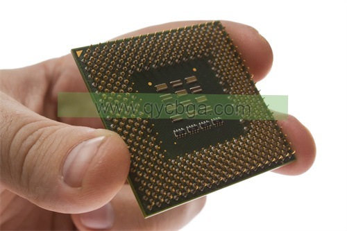
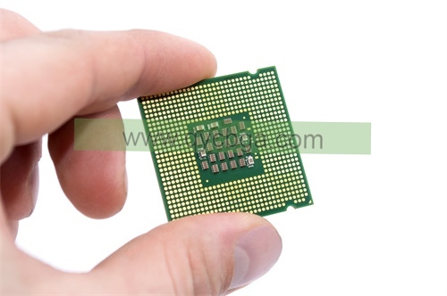
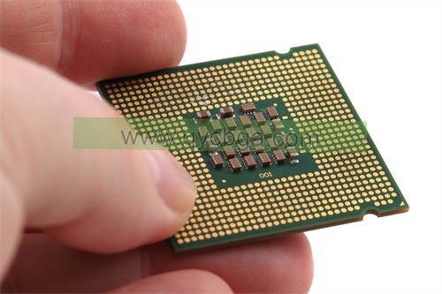
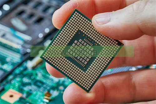
What is SOP Package Substrate?
SOPパッケージ基板メーカー,SOPの (Small Outline Package) package substrate is a compact and streamlined packaging solution widely used in electronic devices where space efficiency is critical. Designed with a small footprint and thin profile, SOP substrates enable high-density mounting on circuit boards, making them ideal for portable electronics such as smartphones, 錠剤, and laptops. These substrates often feature fine pitch interconnects and are made from durable materials such as advanced polymers or ceramics to provide reliable electrical insulation and mechanical strength. The design of SOP package substrates focuses on minimizing package size while maximizing performance, offering enhanced thermal management and reduced signal loss for high-speed applications. This makes SOP an essential choice for designers aiming to optimize functionality in increasingly compact electronic devices.
SOPの (Small Outline Package) is a type of integrated circuit (集積回路) パッケージ that is commonly used for surface-mount devices. It’s a compact and space-saving package designed to be mounted directly onto the surface of a printed circuit board (プリント基板). SOP packages typically have gull-wing or J-lead leads that extend from the sides of the package, allowing for easy soldering onto the PCB.
The substrate of an SOP package refers to the material upon which the integrated circuit is mounted and interconnected. The substrate serves as a foundation for the IC and provides electrical connections between the IC and the external circuitry on the PCB. The substrate material is usually a type of insulating material, such as ceramic or fiberglass, which provides mechanical support and electrical isolation for the IC.
まとめ, the SOP package substrate is the material on which the integrated circuit is mounted within an SOP package, providing structural support and electrical connections for the IC within the package.

SOPパッケージ基板メーカー
SOP Package Substrate design Reference Guide.
The design of the SOPの (Small Outline Package) 基板 is crucial for ensuring the reliable performance and manufacturability of integrated circuits (ICの) mounted within these packages. A comprehensive reference guide for SOP package substrate design typically covers various aspects to consider, 含む:
- 基板材料選定: Discussing the different types of substrate materials available for SOP packages, such as ceramic, ガラス 繊維, or laminate materials. Each material has its own set of characteristics, 熱伝導率を含む, 機械的強度, and cost, which need to be considered based on the specific requirements of the IC and the application.
- Electrical Design Considerations: Providing guidelines for designing the electrical connections (トレース) within the substrate to ensure optimal signal integrity, 配電, と熱管理. This includes considerations for impedance control, power plane distribution, and minimizing parasitic effects such as signal crosstalk and ground bounce.
- サーマルマネジメント: Addressing techniques for managing heat dissipation within the SOP package substrate to prevent overheating of the IC and ensure long-term reliability. This may involve the design of thermal vias, ヒートスプレッダー, and thermal pads to efficiently transfer heat away from the IC to the surrounding environment.
- Mechanical Design Guidelines: Offering recommendations for designing the mechanical aspects of the substrate, including the layout of mounting holes, component clearances, and overall package dimensions. This ensures compatibility with standard assembly processes and mechanical reliability during operation.
- Manufacturability Considerations: Discussing design considerations to facilitate the manufacturing process of SOP package substrates, such as panelization, ソルダーマスク設計, and fiducial marker placement for automated assembly equipment.
- Signal Integrity and EMI Mitigation: Providing guidelines for minimizing signal distortion and electromagnetic interference (EMIの) within the SOP package substrate through proper layout and grounding techniques. This includes considerations for signal routing, デカップリングコンデンサの配置, and shielding strategies.
- Reliability and Testing: Addressing reliability concerns related to the SOP package substrate design, such as solder joint integrity, mechanical stress, と環境要因. Guidelines for reliability testing and qualification of the substrate design may also be included.
By following the recommendations outlined in a comprehensive SOP package substrate design reference guide, designers can optimize the performance, 確実, and manufacturability of ICs mounted within SOP packages for various applications.
What are the materials used in SOP Package Substrate?
The materials used in SOP (Small Outline Package) substrates can vary depending on factors such as cost, performance requirements, と製造プロセス. Some common materials used in SOP package substrates include:
- セラミック: Ceramic substrates offer excellent thermal conductivity and mechanical strength, making them suitable for high-power applications where heat dissipation is critical. アルミナ (Al2O3) および窒化アルミニウム (AlNの) are commonly used ceramic materials for SOP substrates.
- Fiberglass: Fiberglass substrates, also known as FR4 (難燃 4), are composed of a fiberglass-reinforced epoxy laminate. FR4 substrates are cost-effective and widely used in consumer electronics and low- to mid-range applications.
- Laminate: Laminate substrates consist of multiple layers of insulating material, エポキシ樹脂やポリイミドなど, reinforced with fiberglass or other reinforcement materials. Laminate substrates offer good electrical insulation and mechanical properties and are commonly used in SOP packages for various applications.
- ポリイミド: Polyimide substrates offer excellent thermal stability, 柔軟性, and resistance to chemicals and moisture. They are often used in flexible circuits and applications requiring high temperature resistance.
- メタルコア: Metal core substrates feature a layer of metal, アルミニウムや銅など, 絶縁材料の層の間に挟まれている. Metal core substrates provide superior thermal conductivity and are suitable for high-power LED and power electronics applications.
- 銅: Copper substrates offer high thermal conductivity and are commonly used in high-power semiconductor devices and RF (無線周波数) applications where heat dissipation is critical.
These are some of the main materials used in SOP package substrates, each offering unique properties suited to different application requirements. Designers select the substrate material based on factors such as thermal performance, 電気的特性, 費用, and manufacturing feasibility.
How is SOP Package Substrate manufactured?
The manufacturing process for SOP (Small Outline Package) substrates involves several steps to create a durable and functional substrate for mounting integrated circuits (ICの). Below is a general outline of the manufacturing process:
- 基板材料の準備: The process begins with preparing the substrate material, これはセラミックである可能性があります, ガラス 繊維 (FR4の), laminate, メタルコア, または別の適切な材料. The material is typically supplied in sheets or panels of the desired thickness.
- 基板製造: The substrate material undergoes fabrication processes to create the desired shape and dimensions for the SOP package. This may involve cutting, 錬成, and routing the material to form individual substrate units or panels.
- 表面処理: The surface of the substrate material is prepared for subsequent processing steps, such as cleaning to remove contaminants and applying surface treatments or coatings to improve adhesion and solderability.
- Circuit Pattern Formation: このステップの内容, the circuit pattern for interconnecting the ICs and other components is formed on the substrate material. This can be achieved through various techniques such as screen printing, 写真石版, or etching processes, depending on the substrate material and design requirements.
- メタライゼーション: Metal layers are deposited onto the substrate surface to create the conductive traces and pads for electrical connections. Common metals used for metallization include copper, aluminum, と金. The metal deposition process can involve techniques such as sputtering, 電気 めっき, または化学蒸着 (CVD検出器).
- Dielectric Layer Deposition: Insulating layers are deposited or laminated onto the substrate to insulate the conductive traces and provide electrical isolation between layers. These dielectric layers may consist of materials such as epoxy resin, ポリイミド, or other suitable insulating materials.
- ビアフォーメーション: Vias are created in the substrate to allow electrical connections between different layers or to provide thermal pathways for heat dissipation. Vias can be formed using drilling, レーザーアブレーション, or other techniques, followed by metallization to establish electrical continuity.
- 表面仕上げ: The substrate surface is finished to facilitate soldering of ICs and other components during assembly. Common surface finishes include solder mask application, which protects the substrate and defines soldering areas, and surface plating techniques such as electroless nickel immersion gold (エニグ) or hot air solder leveling (ハスレ).
- Quality Control and Testing: 製造プロセス全体を通じて, quality control measures are implemented to ensure the substrate meets specified tolerances and performance criteria. Testing may include visual inspection, 電気試験, and reliability testing to verify the integrity and functionality of the substrates.
- 梱包と配送: Once manufactured and tested, the SOP package substrates are packaged and prepared for shipping to assembly facilities where ICs and other components will be mounted onto them to complete the electronic assemblies.
全, the manufacturing process for SOP package substrates involves a combination of material preparation, 捏造, メタライゼーション, and quality control steps to produce high-quality substrates suitable for use in various electronic applications.
The Application area of SOP Package Substrate
SOPの (Small Outline Package) substrates find applications across a wide range of industries and electronic devices due to their compact size, surface-mount capability, and versatility. Some common application areas of SOP package substrates include:
- 家電: SOP package substrates are extensively used in consumer electronics devices such as smartphones, 錠剤, ラップトップ, デジタルカメラ, およびウェアラブルデバイス. They provide a compact and lightweight solution for mounting integrated circuits (ICの) and other electronic components in these portable devices.
- Telecommunications: SOP substrates are used in telecommunications equipment including routers, スイッチ, modems, and base stations. They facilitate the assembly of high-density electronic circuits with reliable electrical connections, making them suitable for telecommunications infrastructure and networking applications.
- カーエレクトロニクス: 自動車エレクトロニクス, SOP package substrates are employed in various applications such as engine control units (ECU(エキュエート), airbag systems, インフォテインメントシステム, and advanced driver assistance systems (ADASの). They offer robust construction and thermal performance required for harsh automotive environments.
- インダストリアル・オートメーション: SOP package substrates are utilized in industrial automation equipment, 制御システム, ロボティックス, and machinery. They enable the integration of complex electronic circuits with efficient heat dissipation and reliable performance in demanding industrial environments.
- 医療機器: SOP substrates are used in medical devices and equipment such as patient monitoring systems, 診断デバイス, イメージング機器, および医療用インプラント. They provide compact and reliable solutions for mounting sensitive electronic components in medical applications.
- 航空宇宙・防衛: 航空宇宙および防衛用途, SOP package substrates are employed in avionics systems, navigation equipment, レーダーシステム, communications devices, およびミサイル誘導システム. They offer rugged construction, 高い信頼性, and resistance to extreme environmental conditions.
- 再生可能エネルギー: SOP substrates are used in renewable energy systems such as solar inverters, wind turbine controllers, and battery management systems. They enable the efficient integration of power electronics and control circuits for renewable energy generation and storage.
- Consumer Appliances: SOP package substrates find applications in various household appliances including refrigerators, washing machines, dishwashers, microwave ovens, and air conditioners. They provide compact and cost-effective solutions for controlling and monitoring electronic functions in appliances.
全, SOP package substrates play a crucial role in enabling the miniaturization, パフォーマンス, and reliability of electronic devices across a diverse range of industries and applications.
What are the advantages of SOP Package Substrate?
SOPの (Small Outline Package) substrates offer several advantages that make them desirable for a wide range of electronic applications. 主な利点には、次のようなものがあります:
- コンパクトサイズ: SOP packages are designed to be small and compact, making them suitable for space-constrained applications where size is a critical factor. Their small form factor allows for high-density mounting of integrated circuits (ICの) and other components on printed circuit boards (プリント基板), enabling miniaturization of electronic devices.
- Surface-Mount Capability: SOP packages are surface-mountable, meaning they can be directly mounted onto the surface of PCBs without the need for through-holes. This surface-mount capability simplifies the assembly process, reduces manufacturing costs, and enables automated assembly techniques such as pick-and-place machines.
- High Density Integration: SOP substrates support high-density integration of electronic components, ICを含む, resistors, capacitors, and other discrete components. They provide multiple leads or pads for connecting these components, allowing for complex electronic circuits to be implemented in a compact space.
- Good Electrical Performance: SOP substrates offer good electrical performance, including low signal distortion, インピーダンス制御, and reliable electrical connections. The design of SOP packages allows for optimized signal routing and power distribution, contributing to the overall performance and functionality of electronic systems.
- サーマルマネジメント: SOP packages typically feature thermal vias or thermal pads that help dissipate heat generated by ICs during operation. This efficient thermal management ensures reliable performance and prevents overheating of the components, particularly in high-power applications.
- Mechanical Durability: SOP substrates are designed to withstand mechanical stresses and environmental factors encountered during operation, such as shock, 振動, and temperature fluctuations. The robust construction of SOP packages enhances their mechanical durability and reliability in various application environments.
- 費用対効果: SOP packages are often cost-effective compared to other packaging technologies, such as leaded packages or ceramic packages. Their simple design, standardized manufacturing processes, and mass production capabilities contribute to their cost-effectiveness, making them an attractive option for a wide range of electronic devices.
- 互換性: SOP packages are compatible with standard surface-mount assembly processes and equipment, making them easy to integrate into existing manufacturing workflows. They are also compatible with automated testing and inspection methods, ensuring efficient production and quality control.
全, the advantages of SOP package substrates, including their compact size, surface-mount capability, high-density integration, サーマルマネジメント, mechanical durability, そして費用対効果, make them a preferred choice for many electronic applications across various industries.
How Much Does SOP Package Substrate Cost?
The cost of SOP (Small Outline Package) substrates can vary widely depending on several factors, 基板材料を含む, 大きさ, 複雑さ, 量, and manufacturing processes involved. Here are some factors that influence the cost of SOP package substrates:
- 基板材料: The choice of substrate material can significantly impact the cost. 例えば, ceramic substrates tend to be more expensive than fiberglass (FR4の) or laminate substrates due to their superior thermal properties and manufacturing complexity.
- サイズと複雑さ: Larger and more complex SOP substrates with intricate circuit patterns, 複数のレイヤー, and fine-pitch features may require additional manufacturing steps and materials, コストの上昇につながる.
- 量: Economies of scale play a significant role in determining the cost of SOP substrates. Larger production quantities typically result in lower unit costs due to bulk purchasing of materials and increased manufacturing efficiency.
- 製造プロセス: The specific manufacturing processes involved in producing SOP substrates, such as circuit pattern formation, メタライゼーション, via drilling, 表面仕上げ, と品質管理, 全体的なコストに影響を与える可能性があります. Sophisticated manufacturing techniques may incur higher costs compared to simpler processes.
- カスタマイズ: Customized SOP substrates designed to meet specific performance requirements or application needs may incur additional development and setup costs, resulting in higher overall costs compared to standard off-the-shelf substrates.
- サプライヤーとロケーション: The choice of substrate supplier and manufacturing location can also affect the cost. サプライヤーが異なれば、価格体系も異なる場合があります, quality levels, and lead times for SOP substrates.
- 市場環境: Fluctuations in raw material prices, 人件費, and market demand can influence the overall cost of SOP substrates. Supply chain disruptions or shortages of key materials may also impact pricing.
多くの変数が関係しているため, it’s challenging to provide a specific cost for SOP package substrates without knowing the specific requirements of the application and the manufacturing details. 通常, customers can request quotes from substrate suppliers or contract manufacturers based on their exact specifications to determine the cost of SOP substrates for their project.
FAQs about SOP Package Substrate
What is an SOP package substrate?
An SOP package substrate is a type of integrated circuit packaging used to mount and interconnect electronic components, typically smaller and lower-profile than traditional packages. SOP packages are commonly used for small and medium-sized ICs.
What are the advantages of SOP package substrates?
SOP package substrates offer advantages such as compact size, lightweight design, low profile, compatibility with surface mount technology (SMTの), and cost-effectiveness for small and medium-sized electronic components.
What materials are used in SOP package substrates?
Similar to other types of package substrates, materials used in SOP package substrates include substrate core materials (例えば。, FR-4), 導電性トレース用の銅箔, 絶縁用誘電体材料, 保護用ソルダーマスク, and surface finish materials such as immersion tin or gold.
How are SOP package substrates manufactured?
The manufacturing process of SOP package substrates involves similar steps to other package substrates, 基板製造を含む, レイヤーのビルドアップ, 回路形成, 表面仕上げ, と品質管理. しかし, SOP packages typically have simpler designs compared to larger packages.
What are the applications of SOP package substrates?
SOP package substrates are commonly used in various electronic devices where space is limited or where smaller form factors are desired. They are found in applications such as consumer electronics, 電気通信, コンピューティングとネットワーキング, 自動車用電子機器, and industrial electronics.
How much do SOP package substrates cost?
The cost of SOP package substrates can vary depending on factors such as size, 複雑さ, 材料の選択, 製造プロセス, 容積, サプライヤー, と場所. Pricing information can be obtained from substrate manufacturers or suppliers.
Where can I find more information about SOP package substrates?
More information about SOP package substrates can be found through datasheets, アプリケーションノート, 技術記事, 業界出版物, 基板メーカーやサプライヤーとの協議. かつ, online resources and forums may provide insights and discussions related to SOP package substrates.
 FCBGAパッケージ基板メーカー

